参数资料
| 型号: | XC3090L-8PC84C |
| 厂商: | Xilinx Inc |
| 文件页数: | 21/76页 |
| 文件大小: | 0K |
| 描述: | IC FPGA 3.3V C-TEMP 84-PLCC |
| 产品变化通告: | XC3000(L) Discontinuation 01/Feb/2003 |
| 标准包装: | 15 |
| 系列: | XC3000A/L |
| LAB/CLB数: | 320 |
| RAM 位总计: | 64160 |
| 输入/输出数: | 70 |
| 门数: | 6000 |
| 电源电压: | 3 V ~ 3.6 V |
| 安装类型: | 表面贴装 |
| 工作温度: | 0°C ~ 85°C |
| 封装/外壳: | 84-LCC(J 形引线) |
| 供应商设备封装: | 84-PLCC |
第1页第2页第3页第4页第5页第6页第7页第8页第9页第10页第11页第12页第13页第14页第15页第16页第17页第18页第19页第20页当前第21页第22页第23页第24页第25页第26页第27页第28页第29页第30页第31页第32页第33页第34页第35页第36页第37页第38页第39页第40页第41页第42页第43页第44页第45页第46页第47页第48页第49页第50页第51页第52页第53页第54页第55页第56页第57页第58页第59页第60页第61页第62页第63页第64页第65页第66页第67页第68页第69页第70页第71页第72页第73页第74页第75页第76页
R
XC3000 Series Field Programmable Gate Arrays
7-30
November 9, 1998 (Version 3.1)
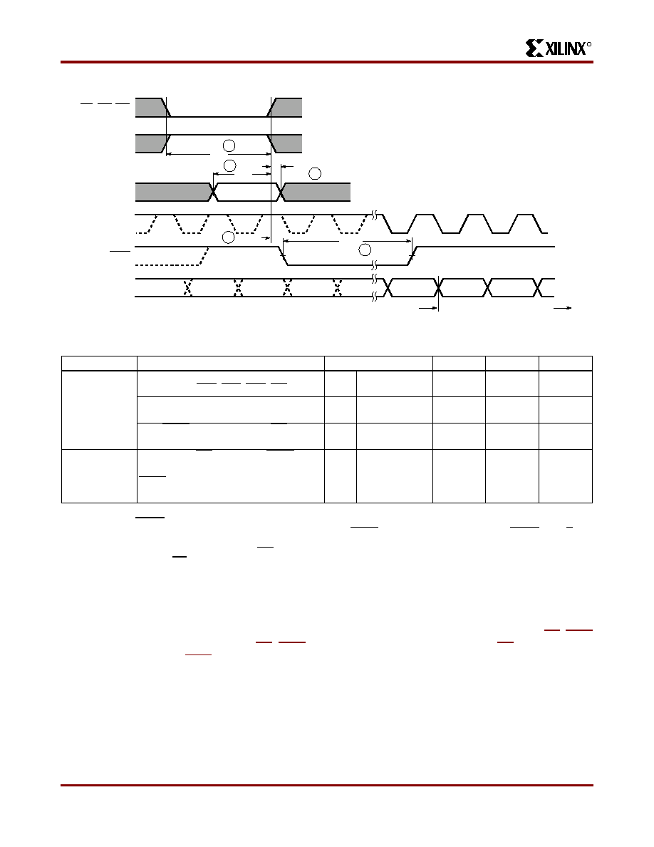
Notes:
1. At power-up, VCC must rise from 2.0 V to VCC min in less than 25 ms. If this is not possible, configuration can be delayed by
holding RESET Low until VCC has reached 4.0 V (2.5 V for the XC3000L). A very long VCC rise time of >100 ms, or a
non-monotonically rising VCC may require a >6-s High level on RESET, followed by a >6-s Low level on RESET and D/P
after VCC has reached 4.0 V (2.5 V for the XC3000L).
2. Configuration must be delayed until the INIT of all FPGAs is High.
3. Time from end of WS to CCLK cycle for the new byte of data depends on completion of previous byte processing and the
phase of the internal timing generator for CCLK.
4. CCLK and DOUT timing is tested in slave mode.
5. TBUSY indicates that the double-buffered parallel-to-serial converter is not yet ready to receive new data. The shortest TBUSY
occurs when a byte is loaded into an empty parallel-to-serial converter. The longest TBUSY occurs when a new word is
loaded into the input register before the second-level buffer has started shifting out data.
Note:
This timing diagram shows very relaxed requirements: Data need not be held beyond the rising edge of WS. BUSY
will go active within 60 ns after the end of WS. BUSY will stay active for several microseconds. WS may be asserted
immediately after the end of BUSY.
Figure 28: Peripheral Mode Programming Switching Characteristics
6
BUSY
T
D6
DOUT
RDY/BUSY
D7
D0
D1
D2
4
WTRB
T
Valid
2
DC
T
1
CA
T
CCLK
D0-D7
CS2
WS, CS0, CS1
3
CD
T
WRITE TO FPGA
X5992
Previous Byte
New Byte
Description
Symbol
Min
Max
Units
WRITE
Effective Write time required
(Assertion of CS0, CS1, CS2, WS)
1TCA
100
ns
DIN Setup time required
DIN Hold time required
2
3
TDC
TCD
60
0
ns
RDY/BUSY delay after end of WS
4TWTRB
60
ns
RDY
Earliest next WS after end of BUSY
5TRBWT
0ns
BUSY Low time generated
6
TBUSY
2.5
9
CCLK
periods
Product Obsolete or Under Obsolescence
相关PDF资料 |
PDF描述 |
|---|---|
| HSC65DRYH-S13 | CONN EDGECARD 130PS .100 EXTEND |
| FMC26DRYI | CONN EDGECARD 52POS DIP .100 SLD |
| ESC50DTES | CONN EDGECARD 100POS .100 EYELET |
| XC3064L-8TQ144I | IC FPGA 3.3V I-TEMP 144-TQFP |
| XC2S100-6FG456C | IC FPGA 2.5V C-TEMP 456-FBGA |
相关代理商/技术参数 |
参数描述 |
|---|---|
| XC3090L-8PC84I | 功能描述:IC FPGA 3.3V I-TEMP 84-PLCC RoHS:否 类别:集成电路 (IC) >> 嵌入式 - FPGA(现场可编程门阵列) 系列:XC3000A/L 产品变化通告:XC4000(E,L) Discontinuation 01/April/2002 标准包装:24 系列:XC4000E/X LAB/CLB数:100 逻辑元件/单元数:238 RAM 位总计:3200 输入/输出数:80 门数:3000 电源电压:4.5 V ~ 5.5 V 安装类型:表面贴装 工作温度:-40°C ~ 100°C 封装/外壳:120-BCBGA 供应商设备封装:120-CPGA(34.55x34.55) |
| XC31 | 制造商:TOREX 制造商全称:Torex Semiconductor 功能描述:Temperature Controlled Voltage Regulators |
| XC3100 | 制造商:XILINX 制造商全称:XILINX 功能描述:Logic Cell Array Families |
| XC3100A | 制造商:XILINX 制造商全称:XILINX 功能描述:Field Programmable Gate Arrays (XC3000A/L, XC3100A/L) |
| XC3100A/L | 制造商:XILINX 制造商全称:XILINX 功能描述:Field Programmable Gate Arrays (XC3000A/L, XC3100A/L) |
发布紧急采购,3分钟左右您将得到回复。