参数资料
| 型号: | XC3090L-8PC84C |
| 厂商: | Xilinx Inc |
| 文件页数: | 75/76页 |
| 文件大小: | 0K |
| 描述: | IC FPGA 3.3V C-TEMP 84-PLCC |
| 产品变化通告: | XC3000(L) Discontinuation 01/Feb/2003 |
| 标准包装: | 15 |
| 系列: | XC3000A/L |
| LAB/CLB数: | 320 |
| RAM 位总计: | 64160 |
| 输入/输出数: | 70 |
| 门数: | 6000 |
| 电源电压: | 3 V ~ 3.6 V |
| 安装类型: | 表面贴装 |
| 工作温度: | 0°C ~ 85°C |
| 封装/外壳: | 84-LCC(J 形引线) |
| 供应商设备封装: | 84-PLCC |
第1页第2页第3页第4页第5页第6页第7页第8页第9页第10页第11页第12页第13页第14页第15页第16页第17页第18页第19页第20页第21页第22页第23页第24页第25页第26页第27页第28页第29页第30页第31页第32页第33页第34页第35页第36页第37页第38页第39页第40页第41页第42页第43页第44页第45页第46页第47页第48页第49页第50页第51页第52页第53页第54页第55页第56页第57页第58页第59页第60页第61页第62页第63页第64页第65页第66页第67页第68页第69页第70页第71页第72页第73页第74页当前第75页第76页
R
XC3000 Series Field Programmable Gate Arrays
7-10
November 9, 1998 (Version 3.1)
Flexible routing allows use of common or individual CLB
clocking.
The combinatorial-logic portion of the CLB uses a 32 by 1
look-up table to implement Boolean functions. Variables
selected from the five logic inputs and two internal block
flip-flops are used as table address inputs. The combinato-
rial propagation delay through the network is independent
of the logic function generated and is spike free for single
input variable changes. This technique can generate two
independent logic functions of up to four variables each as
shown in Figure 6a, or a single function of five variables as
shown in Figure 6b, or some functions of seven variables
as shown in Figure 6c. Figure 7 shows a modulo-8 binary
counter with parallel enable. It uses one CLB of each type.
The partial functions of six or seven variables are imple-
mented using the input variable (E) to dynamically select
between two functions of four different variables. For the
two functions of four variables each, the independent
results (F and G) may be used as data inputs to either
flip-flop or either logic block output. For the single function
of five variables and merged functions of six or seven vari-
ables, the F and G outputs are identical. Symmetry of the F
and G functions and the flip-flops allows the interchange of
CLB outputs to optimize routing efficiencies of the networks
interconnecting the CLBs and IOBs.
Programmable Interconnect
Programmable-interconnection resources in the Field Pro-
grammable Gate Array provide routing paths to connect
inputs and outputs of the IOBs and CLBs into logic net-
works. Interconnections between blocks are composed of a
two-layer grid of metal segments. Specially designed pass
transistors, each controlled by a configuration bit, form pro-
grammable interconnect points (PIPs) and switching matri-
ces used to implement the necessary connections between
selected metal segments and block pins. Figure 8 is an
example of a routed net. The development system provides
automatic routing of these interconnections. Interactive
routing is also available for design optimization. The inputs
of the CLBs or IOBs are multiplexers which can be pro-
grammed to select an input network from the adjacent
interconnect segments.
Since the switch connections to
block inputs are unidirectional, as are block outputs,
they are usable only for block input connection and not
for routing. Figure 9 illustrates routing access to logic
block input variables, control inputs and block outputs.
Three types of metal resources are provided to accommo-
date various network interconnect requirements.
General Purpose Interconnect
Direct Connection
Longlines (multiplexed busses and wide AND gates)
QY
Any Function
of Up to 4
Variables
QY
Any Function
of Up to 4
Variables
QY
Any Function
of 5 Variables
QY
Any Function
of Up to 4
Variables
QY
Any Function
of Up to 4
Variables
5c
5b
5a
QX
A
B
C
D
A
B
C
D
E
A
B
C
D
E
D
A
B
C
D
C
A
B
M
U
X
F
G
F
G
F
G
E
X5442
FGM
Mode
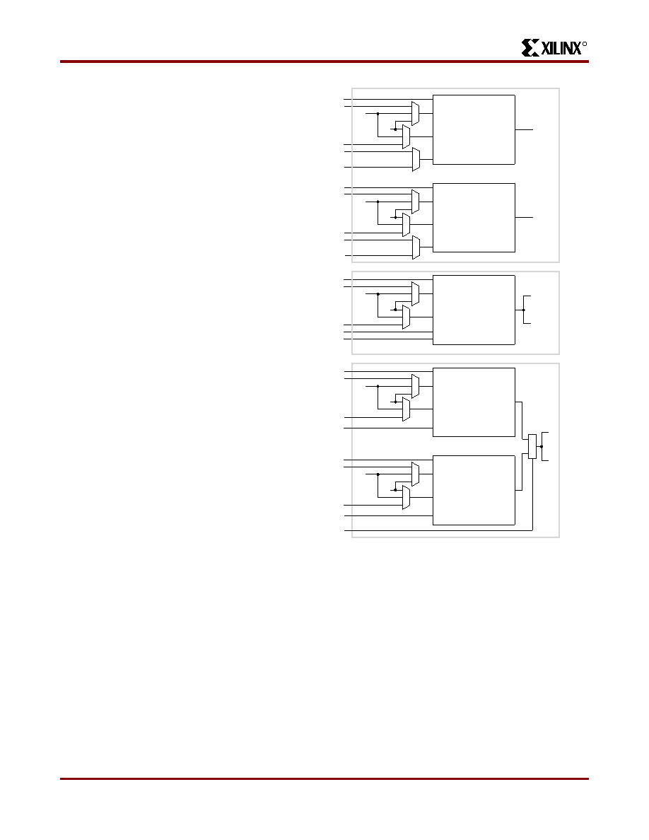
Figure 6: Combinational Logic Options
6a. Combinatorial Logic Option FG generates two func-
tions of four variables each. One variable, A, must be
common to both functions. The second and third variable
can be any choice of B, C, QX and QY. The fourth vari-
able can be any choice of D or E.
6b. Combinatorial Logic Option F generates any function
of five variables: A, D, E and two choices out of B, C, QX,
QY.
6c. Combinatorial Logic Option FGM allows variable E to
select between two functions of four variables: Both have
common inputs A and D and any choice out of B, C, QX
and QY for the remaining two variables. Option 3 can
then implement some functions of six or seven variables.
Product Obsolete or Under Obsolescence
相关PDF资料 |
PDF描述 |
|---|---|
| HSC65DRYH-S13 | CONN EDGECARD 130PS .100 EXTEND |
| FMC26DRYI | CONN EDGECARD 52POS DIP .100 SLD |
| ESC50DTES | CONN EDGECARD 100POS .100 EYELET |
| XC3064L-8TQ144I | IC FPGA 3.3V I-TEMP 144-TQFP |
| XC2S100-6FG456C | IC FPGA 2.5V C-TEMP 456-FBGA |
相关代理商/技术参数 |
参数描述 |
|---|---|
| XC3090L-8PC84I | 功能描述:IC FPGA 3.3V I-TEMP 84-PLCC RoHS:否 类别:集成电路 (IC) >> 嵌入式 - FPGA(现场可编程门阵列) 系列:XC3000A/L 产品变化通告:XC4000(E,L) Discontinuation 01/April/2002 标准包装:24 系列:XC4000E/X LAB/CLB数:100 逻辑元件/单元数:238 RAM 位总计:3200 输入/输出数:80 门数:3000 电源电压:4.5 V ~ 5.5 V 安装类型:表面贴装 工作温度:-40°C ~ 100°C 封装/外壳:120-BCBGA 供应商设备封装:120-CPGA(34.55x34.55) |
| XC31 | 制造商:TOREX 制造商全称:Torex Semiconductor 功能描述:Temperature Controlled Voltage Regulators |
| XC3100 | 制造商:XILINX 制造商全称:XILINX 功能描述:Logic Cell Array Families |
| XC3100A | 制造商:XILINX 制造商全称:XILINX 功能描述:Field Programmable Gate Arrays (XC3000A/L, XC3100A/L) |
| XC3100A/L | 制造商:XILINX 制造商全称:XILINX 功能描述:Field Programmable Gate Arrays (XC3000A/L, XC3100A/L) |
发布紧急采购,3分钟左右您将得到回复。