- 您现在的位置:买卖IC网 > PDF目录205935 > XC5206-3BG225C (Xilinx, Inc.) Field Programmable Gate Arrays PDF资料下载
参数资料
| 型号: | XC5206-3BG225C |
| 厂商: | Xilinx, Inc. |
| 英文描述: | Field Programmable Gate Arrays |
| 中文描述: | 现场可编程门阵列 |
| 文件页数: | 2/73页 |
| 文件大小: | 598K |
| 代理商: | XC5206-3BG225C |
第1页当前第2页第3页第4页第5页第6页第7页第8页第9页第10页第11页第12页第13页第14页第15页第16页第17页第18页第19页第20页第21页第22页第23页第24页第25页第26页第27页第28页第29页第30页第31页第32页第33页第34页第35页第36页第37页第38页第39页第40页第41页第42页第43页第44页第45页第46页第47页第48页第49页第50页第51页第52页第53页第54页第55页第56页第57页第58页第59页第60页第61页第62页第63页第64页第65页第66页第67页第68页第69页第70页第71页第72页第73页
R
XC5200 Series Field Programmable Gate Arrays
7-92
November 5, 1998 (Version 5.2)
non-zero hold, attach a NODELAY attribute or property to
the flip-flop or input buffer.
IOB Output Signals
Output signals can be optionally inverted within the IOB,
and pass directly to the pad. As with the inputs, a CLB
flip-flop or latch can be used to store the output signal.
An active-High 3-state signal can be used to place the out-
put buffer in a high-impedance state, implementing 3-state
outputs or bidirectional I/O. Under configuration control,
the output (OUT) and output 3-state (T) signals can be
inverted.
The polarity of these signals is independently
configured for each IOB.
The XC5200 devices provide a guaranteed output sink cur-
rent of 8 mA.
Supported destinations for XC5200-Series device outputs
are shown in Table 6.(For a detailed discussion of how to
interface between 5 V and 3.3 V devices, see the 3V Prod-
ucts section of
The Programmable Logic Data Book.)
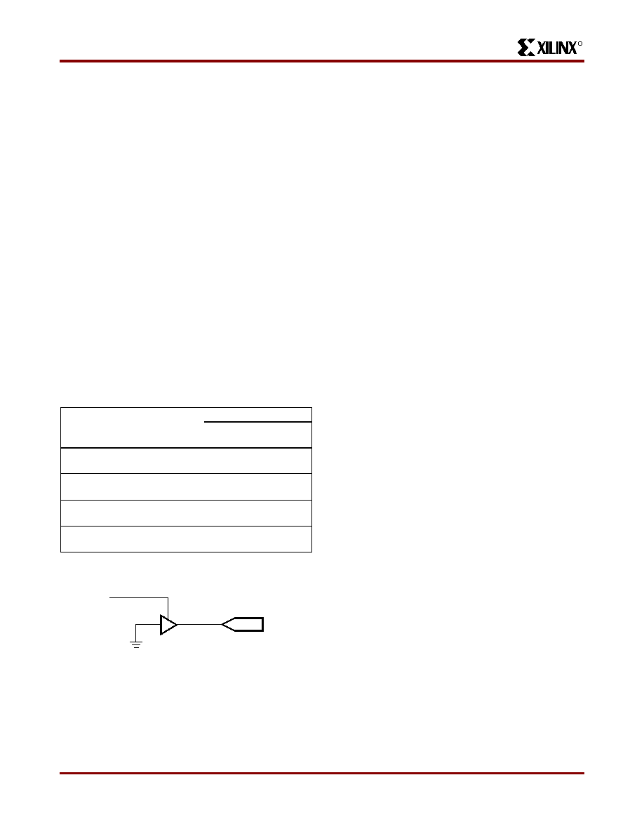
An output can be configured as open-drain (open-collector)
by placing an OBUFT symbol in a schematic or HDL code,
then tying the 3-state pin (T) to the output signal, and the
input pin (I) to Ground. (See Figure 12.)
Table 6: Supported Destinations for XC5200-Series
Outputs
Output Slew Rate
The slew rate of each output buffer is, by default, reduced,
to minimize power bus transients when switching non-criti-
cal signals. For critical signals, attach a FAST attribute or
property to the output buffer or flip-flop.
For XC5200 devices, maximum total capacitive load for
simultaneous fast mode switching in the same direction is
200 pF for all package pins between each Power/Ground
pin pair. For some XC5200 devices, additional internal
Power/Ground pin pairs are connected to special Power
and Ground planes within the packages, to reduce ground
bounce.
For slew-rate limited outputs this total is two times larger for
each device type: 400 pF for XC5200 devices. This maxi-
mum capacitive load should not be exceeded, as it can
result in ground bounce of greater than 1.5 V amplitude and
more than 5 ns duration. This level of ground bounce may
cause undesired transient behavior on an output, or in the
internal logic. This restriction is common to all high-speed
digital ICs, and is not particular to Xilinx or the XC5200
Series.
XC5200-Series devices have a feature called “Soft
Start-up,” designed to reduce ground bounce when all out-
puts are turned on simultaneously at the end of configura-
tion.
When the configuration process is finished and the
device starts up, the first activation of the outputs is auto-
matically slew-rate limited. Immediately following the initial
activation of the I/O, the slew rate of the individual outputs
is determined by the individual configuration option for
each IOB.
Global Three-State
A separate Global 3-State line (not shown in Figure 11)
forces all FPGA outputs to the high-impedance state,
unless boundary scan is enabled and is executing an
EXTEST instruction. This global net (GTS) does not com-
pete with other routing resources; it uses a dedicated distri-
bution network.
GTS can be driven from any user-programmable pin as a
global 3-state input. To use this global net, place an input
pad and input buffer in the schematic or HDL code, driving
the GTS pin of the STARTUP symbol. A specific pin loca-
tion can be assigned to this input using a LOC attribute or
property, just as with any other user-programmable pad. An
inverter can optionally be inserted after the input buffer to
invert the sense of the Global 3-State signal. Using GTS is
similar to Global Reset. See Figure 8 on page 90 for
details. Alternatively, GTS can be driven from any internal
node.
Other IOB Options
There are a number of other programmable options in the
XC5200-Series IOB.
Pull-up and Pull-down Resistors
Programmable IOB pull-up and pull-down resistors are
useful for tying unused pins to Vcc or Ground to minimize
power consumption and reduce noise sensitivity. The con-
figurable pull-up resistor is a p-channel transistor that pulls
Destination
XC5200 Output Mode
5 V,
CMOS
XC5200 device, VCC=3.3 V,
CMOS-threshold inputs
√
Any typical device, VCC = 3.3 V,
CMOS-threshold inputs
some1
1. Only if destination device has 5-V tolerant inputs
Any device, VCC = 5 V,
TTL-threshold inputs
√
Any device, VCC = 5 V,
CMOS-threshold inputs
√
X6702
OPAD
OBUFT
Figure 12: Open-Drain Output
相关PDF资料 |
PDF描述 |
|---|---|
| XC5206-3BG352C | Field Programmable Gate Arrays |
| XC5206-3HQ208C | Field Programmable Gate Arrays |
| XC5206-3HQ240C | Field Programmable Gate Arrays |
| XC5206-3PG156C | Field Programmable Gate Arrays |
| XC5206-3PG223C | Field Programmable Gate Arrays |
相关代理商/技术参数 |
参数描述 |
|---|---|
| XC5206-3BG352C | 制造商:XILINX 制造商全称:XILINX 功能描述:Field Programmable Gate Arrays |
| XC5206-3HQ208C | 制造商:XILINX 制造商全称:XILINX 功能描述:Field Programmable Gate Arrays |
| XC5206-3HQ240C | 制造商:XILINX 制造商全称:XILINX 功能描述:Field Programmable Gate Arrays |
| XC5206-3PC84C | 制造商:Xilinx 功能描述: |
| XC5206-3PC84I | 制造商:未知厂家 制造商全称:未知厂家 功能描述:Field Programmable Gate Array (FPGA) |
发布紧急采购,3分钟左右您将得到回复。