- 您现在的位置:买卖IC网 > PDF目录205935 > XC5206-3BG225C (Xilinx, Inc.) Field Programmable Gate Arrays PDF资料下载
参数资料
| 型号: | XC5206-3BG225C |
| 厂商: | Xilinx, Inc. |
| 英文描述: | Field Programmable Gate Arrays |
| 中文描述: | 现场可编程门阵列 |
| 文件页数: | 73/73页 |
| 文件大小: | 598K |
| 代理商: | XC5206-3BG225C |
第1页第2页第3页第4页第5页第6页第7页第8页第9页第10页第11页第12页第13页第14页第15页第16页第17页第18页第19页第20页第21页第22页第23页第24页第25页第26页第27页第28页第29页第30页第31页第32页第33页第34页第35页第36页第37页第38页第39页第40页第41页第42页第43页第44页第45页第46页第47页第48页第49页第50页第51页第52页第53页第54页第55页第56页第57页第58页第59页第60页第61页第62页第63页第64页第65页第66页第67页第68页第69页第70页第71页第72页当前第73页
R
November 5, 1998 (Version 5.2)
7-91
XC5200 Series Field Programmable Gate Arrays
7
Input/Output Blocks
User-configurable input/output blocks (IOBs) provide the
interface between external package pins and the internal
logic. Each IOB controls one package pin and can be con-
figured for input, output, or bidirectional signals.
The I/O block, shown in Figure 11, consists of an input
buffer and an output buffer. The output driver is an 8-mA
full-rail CMOS buffer with 3-state control. Two slew-rate
control modes are supported to minimize bus transients.
Both the output buffer and the 3-state control are invertible.
The input buffer has globally selected CMOS or TTL input
thresholds. The input buffer is invertible and also provides a
programmable delay line to assure reliable chip-to-chip
set-up and hold times. Minimum ESD protection is 3 KV
using the Human Body Model.
IOB Input Signals
The XC5200 inputs can be globally configured for either
TTL (1.2V) or CMOS thresholds, using an option in the bit-
stream generation software. There is a slight hysteresis of
about 300mV.
The inputs of XC5200-Series 5-Volt devices can be driven
by the outputs of any 3.3-Volt device, if the 5-Volt inputs are
in TTL mode.
Supported sources for XC5200-Series device inputs are
shown in Table 5.
Optional Delay Guarantees Zero Hold Time
XC5200 devices do not have storage elements in the IOBs.
However, XC5200 IOBs can be efficiently routed to CLB
flip-flops or latches to store the I/O signals.
The data input to the register can optionally be delayed by
several nanoseconds. With the delay enabled, the setup
time of the input flip-flop is increased so that normal clock
routing does not result in a positive hold-time requirement.
A positive hold time requirement can lead to unreliable,
temperature- or processing-dependent operation.
The input flip-flop setup time is defined between the data
measured at the device I/O pin and the clock input at the
CLB (not at the clock pin).
Any routing delay from the
device clock pin to the clock input of the CLB must, there-
fore, be subtracted from this setup time to arrive at the real
setup time requirement relative to the device pins. A short
specified setup time might, therefore, result in a negative
setup time at the device pins, i.e., a positive hold-time
requirement.
When a delay is inserted on the data line, more clock delay
can be tolerated without causing a positive hold-time
requirement. Sufficient delay eliminates the possibility of a
data hold-time requirement at the external pin. The maxi-
mum delay is therefore inserted as the software default.
The XC5200 IOB has a one-tap delay element: either the
delay is inserted (default), or it is not. The delay guarantees
a zero hold time with respect to clocks routed through any
of the XC5200 global clock buffers. (See “Global Lines” on
page 96 for a description of the global clock buffers in the
XC5200.) For a shorter input register setup time, with
D
N
D
C
D
B
D
A
AB
C
N
Z = D
A
A + D
B
B + D
C
C + D
N
N
~100 k
"Weak Keeper"
X6466
BUFT
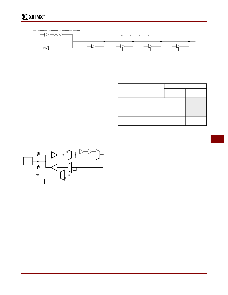
Figure 10: 3-State Buffers Implement a Multiplexer
Figure 11: XC5200 I/O Block
I
O
T
PAD
Vcc
X9001
Input
Buffer
Delay
Pullup
Pulldown
Slew Rate
Control
Output
Buffer
Table 5: Supported Sources for XC5200-Series Device
Inputs
Source
XC5200 Input Mode
5 V,
TTL
5 V,
CMOS
Any device, Vcc = 3.3 V,
CMOS outputs
√
Unreliable
Data
Any device, Vcc = 5 V,
TTL outputs
√
Any device, Vcc = 5 V,
CMOS outputs
√√
相关PDF资料 |
PDF描述 |
|---|---|
| XC5206-3BG352C | Field Programmable Gate Arrays |
| XC5206-3HQ208C | Field Programmable Gate Arrays |
| XC5206-3HQ240C | Field Programmable Gate Arrays |
| XC5206-3PG156C | Field Programmable Gate Arrays |
| XC5206-3PG223C | Field Programmable Gate Arrays |
相关代理商/技术参数 |
参数描述 |
|---|---|
| XC5206-3BG352C | 制造商:XILINX 制造商全称:XILINX 功能描述:Field Programmable Gate Arrays |
| XC5206-3HQ208C | 制造商:XILINX 制造商全称:XILINX 功能描述:Field Programmable Gate Arrays |
| XC5206-3HQ240C | 制造商:XILINX 制造商全称:XILINX 功能描述:Field Programmable Gate Arrays |
| XC5206-3PC84C | 制造商:Xilinx 功能描述: |
| XC5206-3PC84I | 制造商:未知厂家 制造商全称:未知厂家 功能描述:Field Programmable Gate Array (FPGA) |
发布紧急采购,3分钟左右您将得到回复。