- 您现在的位置:买卖IC网 > PDF目录205935 > XC5206-3BG225C (Xilinx, Inc.) Field Programmable Gate Arrays PDF资料下载
参数资料
| 型号: | XC5206-3BG225C |
| 厂商: | Xilinx, Inc. |
| 英文描述: | Field Programmable Gate Arrays |
| 中文描述: | 现场可编程门阵列 |
| 文件页数: | 8/73页 |
| 文件大小: | 598K |
| 代理商: | XC5206-3BG225C |
第1页第2页第3页第4页第5页第6页第7页当前第8页第9页第10页第11页第12页第13页第14页第15页第16页第17页第18页第19页第20页第21页第22页第23页第24页第25页第26页第27页第28页第29页第30页第31页第32页第33页第34页第35页第36页第37页第38页第39页第40页第41页第42页第43页第44页第45页第46页第47页第48页第49页第50页第51页第52页第53页第54页第55页第56页第57页第58页第59页第60页第61页第62页第63页第64页第65页第66页第67页第68页第69页第70页第71页第72页第73页
R
XC5200 Series Field Programmable Gate Arrays
7-98
November 5, 1998 (Version 5.2)
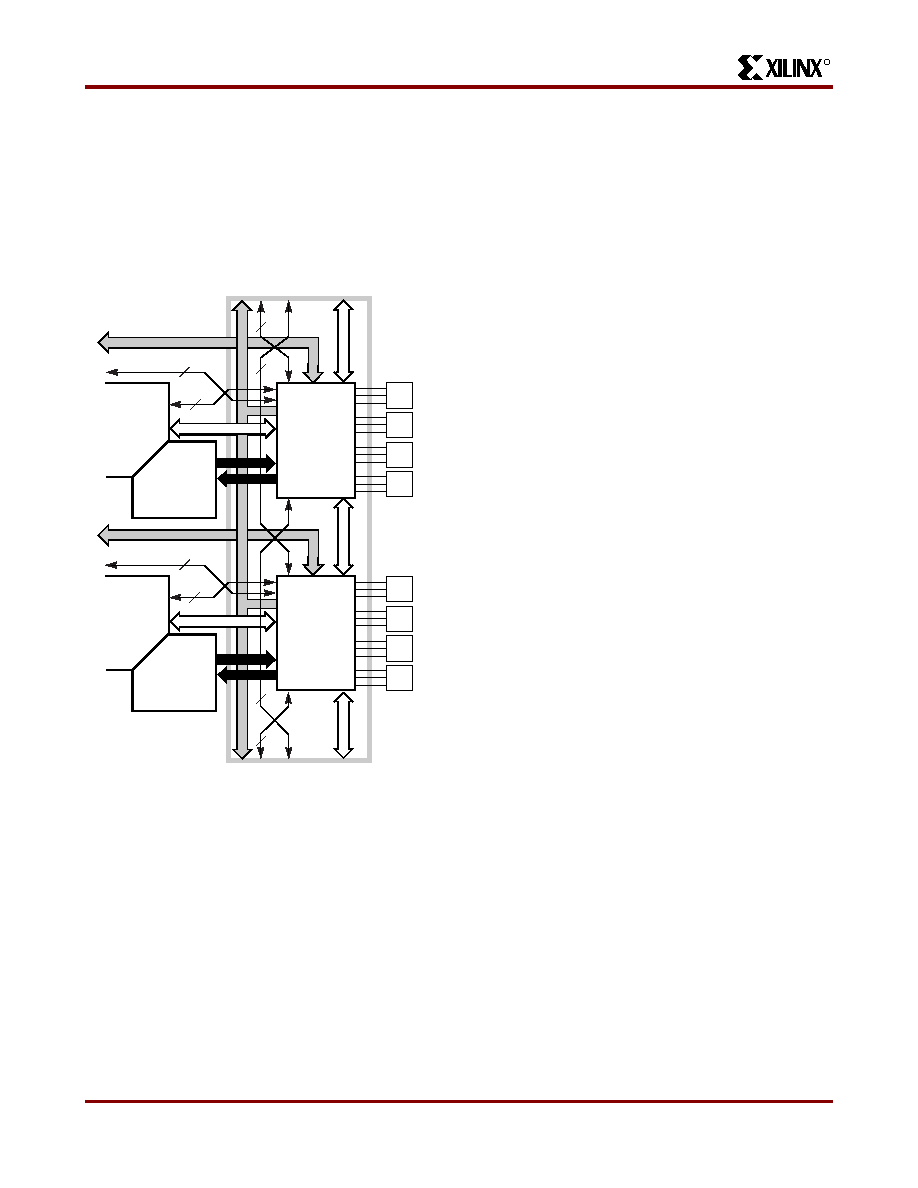
VersaRing Input/Output Interface
The VersaRing, shown in Figure 18, is positioned between
the core logic and the pad ring; it has all the routing
resources of a VersaBlock without the CLB logic. The Ver-
saRing decouples the core logic from the I/O pads. Each
VersaRing Cell provides up to four pad-cell connections on
one side, and connects directly to the CLB ports on the
other side.
Boundary Scan
The “bed of nails” has been the traditional method of testing
electronic assemblies. This approach has become less
appropriate, due to closer pin spacing and more sophisti-
cated assembly methods like surface-mount technology
and multi-layer boards. The IEEE boundary scan standard
1149.1 was developed to facilitate board-level testing of
electronic assemblies. Design and test engineers can
imbed a standard test logic structure in their device to
achieve high fault coverage for I/O and internal logic. This
structure is easily implemented with a four-pin interface on
any boundary scan-compatible IC. IEEE 1149.1-compatible
devices may be serial daisy-chained together, connected in
parallel, or a combination of the two.
XC5200 devices support all the mandatory boundary-scan
instructions specified in the IEEE standard 1149.1. A Test
Access Port (TAP) and registers are provided that imple-
ment the EXTEST, SAMPLE/PRELOAD, and BYPASS
instructions. The TAP can also support two USERCODE
instructions. When the boundary scan configuration option
is selected, three normal user I/O pins become dedicated
inputs for these functions. Another user output pin
becomes the dedicated boundary scan output.
Boundary-scan operation is independent of individual IOB
configuration and package type. All IOBs are treated as
independently controlled bidirectional pins, including any
unbonded IOBs. Retaining the bidirectional test capability
after configuration provides flexibility for interconnect test-
ing.
Also, internal signals can be captured during EXTEST by
connecting them to unbonded IOBs, or to the unused out-
puts in IOBs used as unidirectional input pins. This tech-
nique partially compensates for the lack of INTEST
support.
The user can serially load commands and data into these
devices to control the driving of their outputs and to exam-
ine their inputs. This method is an improvement over
bed-of-nails testing. It avoids the need to over-drive device
outputs, and it reduces the user interface to four pins. An
optional fifth pin, a reset for the control logic, is described in
the standard but is not implemented in Xilinx devices.
The dedicated on-chip logic implementing the IEEE 1149.1
functions includes a 16-state machine, an instruction regis-
ter and a number of data registers. The functional details
can be found in the IEEE 1149.1 specification and are also
discussed in the Xilinx application note XAPP 017:
“Bound-
ary Scan in XC4000 and XC5200 Series devices”
Figure 19 on page 99 is a diagram of the XC5200-Series
boundary scan logic. It includes three bits of Data Register
per IOB, the IEEE 1149.1 Test Access Port controller, and
the Instruction Register with decodes.
The public boundary-scan instructions are always available
prior to configuration. After configuration, the public instruc-
tions and any USERCODE instructions are only available if
specified in the design. While SAMPLE and BYPASS are
available during configuration, it is recommended that
boundary-scan operations not be performed during this
transitory period.
In addition to the test instructions outlined above, the
boundary-scan circuitry can be used to configure the FPGA
device, and to read back the configuration data.
All of the XC4000 boundary-scan modes are supported in
the XC5200 family. Three additional outputs for the User-
Register are provided (Reset, Update, and Shift), repre-
Figure 18: VersaRing I/O Interface
8
GRM
VersaBlock
8
VersaRing
2
4
8
4
10
2
GRM
VersaBlock
8
2
8
10
Interconnect
Pad
X5705
相关PDF资料 |
PDF描述 |
|---|---|
| XC5206-3BG352C | Field Programmable Gate Arrays |
| XC5206-3HQ208C | Field Programmable Gate Arrays |
| XC5206-3HQ240C | Field Programmable Gate Arrays |
| XC5206-3PG156C | Field Programmable Gate Arrays |
| XC5206-3PG223C | Field Programmable Gate Arrays |
相关代理商/技术参数 |
参数描述 |
|---|---|
| XC5206-3BG352C | 制造商:XILINX 制造商全称:XILINX 功能描述:Field Programmable Gate Arrays |
| XC5206-3HQ208C | 制造商:XILINX 制造商全称:XILINX 功能描述:Field Programmable Gate Arrays |
| XC5206-3HQ240C | 制造商:XILINX 制造商全称:XILINX 功能描述:Field Programmable Gate Arrays |
| XC5206-3PC84C | 制造商:Xilinx 功能描述: |
| XC5206-3PC84I | 制造商:未知厂家 制造商全称:未知厂家 功能描述:Field Programmable Gate Array (FPGA) |
发布紧急采购,3分钟左右您将得到回复。