- 您现在的位置:买卖IC网 > PDF目录205935 > XC5206-3BG225C (Xilinx, Inc.) Field Programmable Gate Arrays PDF资料下载
参数资料
| 型号: | XC5206-3BG225C |
| 厂商: | Xilinx, Inc. |
| 英文描述: | Field Programmable Gate Arrays |
| 中文描述: | 现场可编程门阵列 |
| 文件页数: | 67/73页 |
| 文件大小: | 598K |
| 代理商: | XC5206-3BG225C |
第1页第2页第3页第4页第5页第6页第7页第8页第9页第10页第11页第12页第13页第14页第15页第16页第17页第18页第19页第20页第21页第22页第23页第24页第25页第26页第27页第28页第29页第30页第31页第32页第33页第34页第35页第36页第37页第38页第39页第40页第41页第42页第43页第44页第45页第46页第47页第48页第49页第50页第51页第52页第53页第54页第55页第56页第57页第58页第59页第60页第61页第62页第63页第64页第65页第66页当前第67页第68页第69页第70页第71页第72页第73页
R
November 5, 1998 (Version 5.2)
7-89
XC5200 Series Field Programmable Gate Arrays
7
tomized RPMs, freeing the designer from the need to
become an expert on architectures.
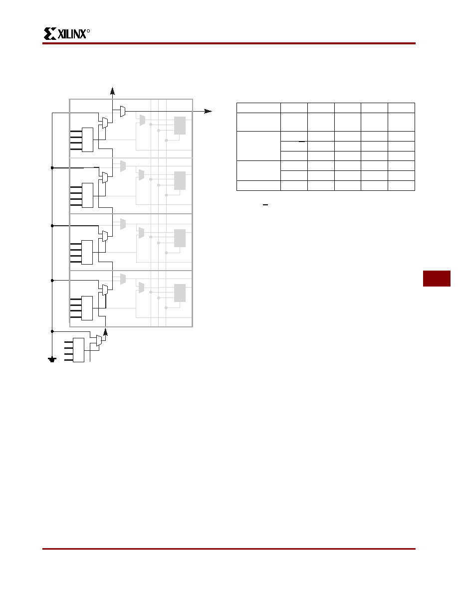
Cascade Function
Each CY_MUX can be connected to the CY_MUX in the
adjacent LC to provide cascadable decode logic. Figure 7
illustrates how the 4-input function generators can be con-
figured to take advantage of these four cascaded
CY_MUXes. Note that AND and OR cascading are specific
cases of a general decode. In AND cascading all bits are
decoded equal to logic one, while in OR cascading all bits
are decoded equal to logic zero. The flexibility of the LUT
achieves this result. The XC5200 library contains gate
macros designed to take advantage of this function.
CLB Flip-Flops and Latches
The CLB can pass the combinatorial output(s) to the inter-
connect network, but can also store the combinatorial
results or other incoming data in flip-flops, and connect
their outputs to the interconnect network as well. The CLB
storage elements can also be configured as latches.
Data Inputs and Outputs
The source of a storage element data input is programma-
ble. It is driven by the function F, or by the Direct In (DI)
block input. The flip-flops or latches drive the Q CLB out-
puts.
Four fast feed-through paths from DI to DO are available,
as shown in Figure 4. This bypass is sometimes used by
the automated router to repower internal signals. In addi-
tion to the storage element (Q) and direct (DO) outputs,
there is a combinatorial output (X) that is always sourced
by the Lookup Table.
The four edge-triggered D-type flip-flops or level-sensitive
latches have common clock (CK) and clock enable (CE)
inputs. Any of the clock inputs can also be permanently
enabled. Storage element functionality is described in
Clock Input
The flip-flops can be triggered on either the rising or falling
clock edge. The clock pin is shared by all four storage ele-
ments with individual polarity control. Any inverter placed
on the clock input is automatically absorbed into the CLB.
Clock Enable
The clock enable signal (CE) is active High. The CE pin is
shared by the four storage elements. If left unconnected
for any, the clock enable for that storage element defaults
to the active state. CE is not invertible within the CLB.
Clear
An asynchronous storage element input (CLR) can be used
to reset all four flip-flops or latches in the CLB. This input
Figure 7: XC5200 CY_MUX Used for Decoder Cascade
Logic
F4
F3
F2
F1
F4
F3
F2
F1
F4
F3
F2
F1
F4
F3
F2
F1
A15
A14
A13
A12
A11
A10
A9
A8
A7
A6
A5
A4
A3
A2
A1
A0
AND
F=0
DI
FD
cascade out
out
DO
D
X
LC3
DO
DQ
LC2
X
CI
cascade in
CY_MUX
FD
X
LC1
Initialization of
carry chain (One Logic Cell)
LC0
CK
CE
CLR
D
Q
X
Q
CO
AND
X5708
Table 3: CLB Storage Element Functionality
(active rising edge is shown)
Mode
CK
CE
CLR
D
Q
Power-Up or
GR
XXXX
0
Flip-Flop
XX
1
X
0
__/
1*
0*
D
0X
0*
X
Q
Latch
11*
0*
X
Q
01*
0*
D
Both
X
0
0*
X
Q
Legend:
X
__/
0*
1*
Don’t care
Rising edge
Input is Low or unconnected (default value)
Input is High or unconnected (default value)
相关PDF资料 |
PDF描述 |
|---|---|
| XC5206-3BG352C | Field Programmable Gate Arrays |
| XC5206-3HQ208C | Field Programmable Gate Arrays |
| XC5206-3HQ240C | Field Programmable Gate Arrays |
| XC5206-3PG156C | Field Programmable Gate Arrays |
| XC5206-3PG223C | Field Programmable Gate Arrays |
相关代理商/技术参数 |
参数描述 |
|---|---|
| XC5206-3BG352C | 制造商:XILINX 制造商全称:XILINX 功能描述:Field Programmable Gate Arrays |
| XC5206-3HQ208C | 制造商:XILINX 制造商全称:XILINX 功能描述:Field Programmable Gate Arrays |
| XC5206-3HQ240C | 制造商:XILINX 制造商全称:XILINX 功能描述:Field Programmable Gate Arrays |
| XC5206-3PC84C | 制造商:Xilinx 功能描述: |
| XC5206-3PC84I | 制造商:未知厂家 制造商全称:未知厂家 功能描述:Field Programmable Gate Array (FPGA) |
发布紧急采购,3分钟左右您将得到回复。