参数资料
| 型号: | XC6VCX130T-2FFG784C |
| 厂商: | Xilinx Inc |
| 文件页数: | 24/52页 |
| 文件大小: | 0K |
| 描述: | IC FPGA VIRTEX 6 128K 784FFGBGA |
| 产品培训模块: | Virtex-6 FPGA Overview |
| 产品变化通告: | Virtex-6 FIFO Input Logic Reset 18/Apr/2011 |
| 标准包装: | 1 |
| 系列: | Virtex® 6 CXT |
| LAB/CLB数: | 10000 |
| 逻辑元件/单元数: | 128000 |
| RAM 位总计: | 9732096 |
| 输入/输出数: | 400 |
| 电源电压: | 0.95 V ~ 1.05 V |
| 安装类型: | 表面贴装 |
| 工作温度: | 0°C ~ 85°C |
| 封装/外壳: | 784-BBGA,FCBGA |
| 供应商设备封装: | 784-FCBGA |
第1页第2页第3页第4页第5页第6页第7页第8页第9页第10页第11页第12页第13页第14页第15页第16页第17页第18页第19页第20页第21页第22页第23页当前第24页第25页第26页第27页第28页第29页第30页第31页第32页第33页第34页第35页第36页第37页第38页第39页第40页第41页第42页第43页第44页第45页第46页第47页第48页第49页第50页第51页第52页
Virtex-6 CXT Family Data Sheet
DS153 (v1.6) February 11, 2011
Product Specification
30
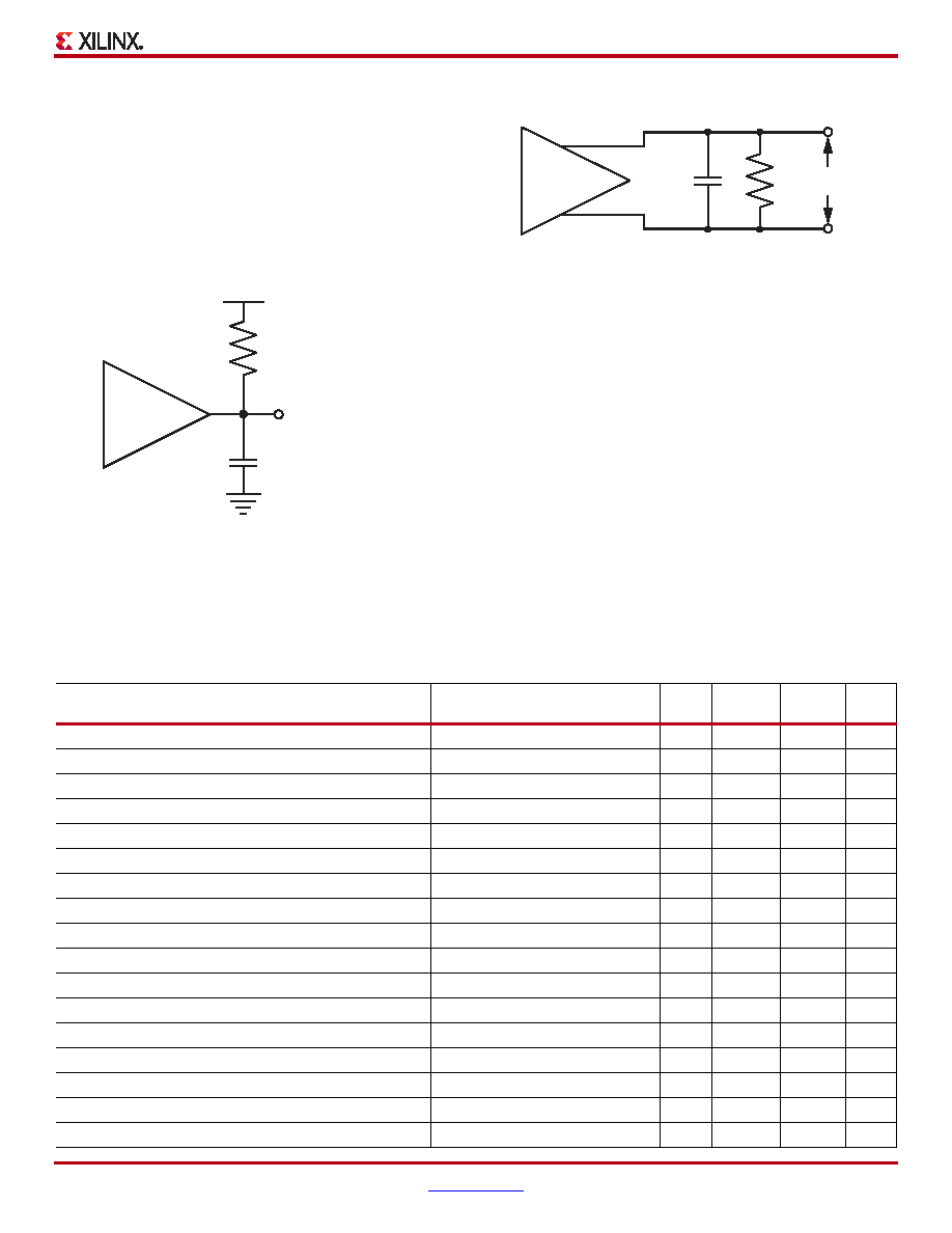
Output Delay Measurements
Output delays are measured using a Tektronix P6245
TDS500/600 probe (< 1 pF) across approximately 4" of FR4
microstrip trace. Standard termination was used for all
testing. The propagation delay of the 4" trace is
characterized separately and subtracted from the final
measurement, and is therefore not included in the
Measurements and test conditions are reflected in the IBIS
models except where the IBIS format precludes it.
Parameters VREF, RREF, CREF, and VMEAS fully describe
the test conditions for each I/O standard. The most accurate
prediction of propagation delay in any given application can
be obtained through IBIS simulation, using the following
method:
1.
Simulate the output driver of choice into the generalized
test setup, using values from Table 41.
2.
Record the time to VMEAS.
3.
Simulate the output driver of choice into the actual PCB
trace and load, using the appropriate IBIS model or
capacitance value to represent the load.
4.
Record the time to VMEAS.
5.
decrease in delay yields the actual propagation delay of
the PCB trace.
X-Ref Target - Figure 14
Figure 14: Single Ended Test Setup
VREF
RREF
VMEAS
(voltage level when taking
delay measurement)
CREF
(probe capacitance)
FPGA Output
ds152_06_042109
X-Ref Target - Figure 15
Figure 15: Differential Test Setup
RREF VMEAS
+
–
CREF
FPGA Output
ds152_07_042109
Table 41: Output Delay Measurement Methodology
Description
I/O Standard
Attribute
RREF
(
)
CREF(1)
(pF)
VMEAS
(V)
VREF
(V)
LVCMOS, 2.5V
LVCMOS25
1M
0
1.25
0
LVCMOS, 1.8V
LVCMOS18
1M
0
0.9
0
LVCMOS, 1.5V
LVCMOS15
1M
0
0.75
0
LVCMOS, 1.2V
LVCMOS12
1M
0
0.75
0
HSTL (High-Speed Transceiver Logic), Class I
HSTL_I
50
0
VREF
0.75
HSTL, Class II
HSTL_II
25
0
VREF
0.75
HSTL, Class III
HSTL_III
50
0
0.9
1.5
HSTL, Class I, 1.8V
HSTL_I_18
50
0
VREF
0.9
HSTL, Class II, 1.8V
HSTL_II_18
25
0
VREF
0.9
HSTL, Class III, 1.8V
HSTL_III_18
50
0
1.1
1.8
SSTL (Stub Series Terminated Logic), Class I, 1.8V
SSTL18_I
50
0
VREF
0.9
SSTL, Class II, 1.8V
SSTL18_II
25
0
VREF
0.9
SSTL, Class I, 2.5V
SSTL2_I
50
0
VREF
1.25
SSTL, Class II, 2.5V
SSTL2_II
25
0
VREF
1.25
LVDS (Low-Voltage Differential Signaling), 2.5V
LVDS_25
100
0
0(2)
1.2
LVDSEXT (LVDS Extended Mode), 2.5V
LVDS_25
100
0
1.2
BLVDS (Bus LVDS), 2.5V
BLVDS_25
100
0
0
相关PDF资料 |
PDF描述 |
|---|---|
| XC4VLX60-10FF668I | IC FPGA VIRTEX-4LX 668FFBGA |
| XC6VLX75T-L1FFG784C | IC FPGA VIRTEX 6 74K 784FFGBGA |
| XCV400E-8FG676C | IC FPGA 1.8V C-TEMP 676-FBGA |
| XCV400E-8BG560C | IC FPGA 1.8V C-TEMP 560-MBGA |
| BR25L010FV-WE2 | IC EEPROM SER 1KB SPI BUS 8SSOP |
相关代理商/技术参数 |
参数描述 |
|---|---|
| XC6VCX130T-2FFG784I | 功能描述:IC FPGA VIRTEX 6 128K 784FFGBGA RoHS:是 类别:集成电路 (IC) >> 嵌入式 - FPGA(现场可编程门阵列) 系列:Virtex® 6 CXT 产品变化通告:Step Intro and Pkg Change 11/March/2008 标准包装:1 系列:Virtex®-5 SXT LAB/CLB数:4080 逻辑元件/单元数:52224 RAM 位总计:4866048 输入/输出数:480 门数:- 电源电压:0.95 V ~ 1.05 V 安装类型:表面贴装 工作温度:-40°C ~ 100°C 封装/外壳:1136-BBGA,FCBGA 供应商设备封装:1136-FCBGA 配用:568-5088-ND - BOARD DEMO DAC1408D750122-1796-ND - EVALUATION PLATFORM VIRTEX-5 |
| XC6VCX195T | 制造商:XILINX 制造商全称:XILINX 功能描述:Virtex-6 CXT Family Data Sheet |
| XC6VCX195T-1FF1156C | 制造商:Xilinx 功能描述:FPGA VIRTEX?-6 CXT FAMILY 199680 CELLS 40NM (CMOS) TECHNOLOG - Trays 制造商:Xilinx 功能描述:IC FPGA VIRTEX 6 195K 1156BGA |
| XC6VCX195T-1FF1156I | 制造商:Xilinx 功能描述:FPGA VIRTEX?-6 CXT FAMILY 199680 CELLS 40NM (CMOS) TECHNOLOG - Trays 制造商:Xilinx 功能描述:IC FPGA VIRTEX 6 195K 1156BGA |
| XC6VCX195T-1FF784C | 制造商:Xilinx 功能描述:FPGA VIRTEX?-6 CXT FAMILY 199680 CELLS 40NM (CMOS) TECHNOLOG - Trays 制造商:Xilinx 功能描述:IC FPGA VIRTEX 6 195K 784BGA |
发布紧急采购,3分钟左右您将得到回复。