参数资料
| 型号: | XC6VCX130T-2FFG784C |
| 厂商: | Xilinx Inc |
| 文件页数: | 9/52页 |
| 文件大小: | 0K |
| 描述: | IC FPGA VIRTEX 6 128K 784FFGBGA |
| 产品培训模块: | Virtex-6 FPGA Overview |
| 产品变化通告: | Virtex-6 FIFO Input Logic Reset 18/Apr/2011 |
| 标准包装: | 1 |
| 系列: | Virtex® 6 CXT |
| LAB/CLB数: | 10000 |
| 逻辑元件/单元数: | 128000 |
| RAM 位总计: | 9732096 |
| 输入/输出数: | 400 |
| 电源电压: | 0.95 V ~ 1.05 V |
| 安装类型: | 表面贴装 |
| 工作温度: | 0°C ~ 85°C |
| 封装/外壳: | 784-BBGA,FCBGA |
| 供应商设备封装: | 784-FCBGA |
第1页第2页第3页第4页第5页第6页第7页第8页当前第9页第10页第11页第12页第13页第14页第15页第16页第17页第18页第19页第20页第21页第22页第23页第24页第25页第26页第27页第28页第29页第30页第31页第32页第33页第34页第35页第36页第37页第38页第39页第40页第41页第42页第43页第44页第45页第46页第47页第48页第49页第50页第51页第52页
Virtex-6 CXT Family Data Sheet
DS153 (v1.6) February 11, 2011
Product Specification
17
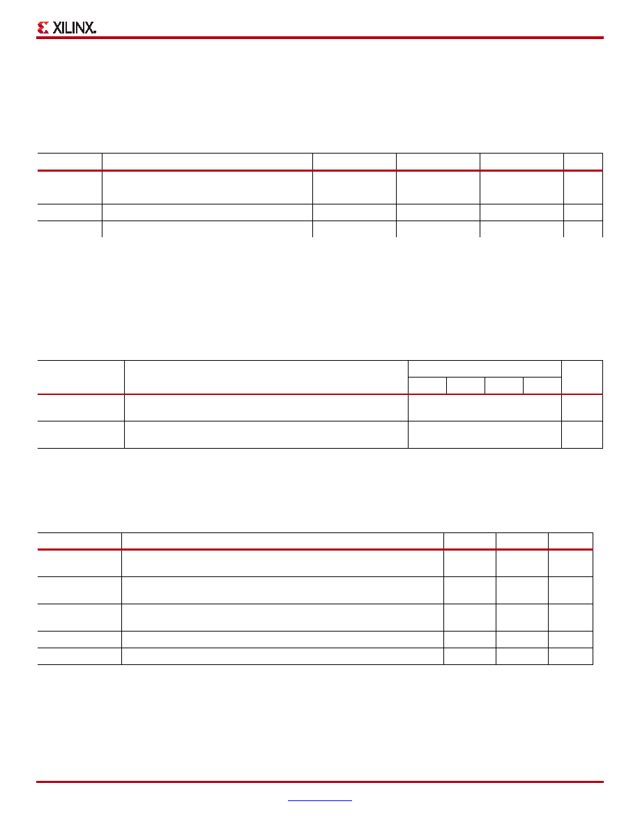
LVPECL DC Specifications (LVPECL_25)
These values are valid when driving a 100
differential load only, i.e., a 100 resistor between the two receiver pins. The
VOH levels are 200 mV below standard LVPECL levels and are compatible with devices tolerant of lower common-mode
ranges. Table 19 summarizes the DC output specifications of LVPECL. For more information on using LVPECL
, see the
Virtex-6 FPGA SelectIO Resources User Guide.
eFUSE Read Endurance
Table 20 lists the maximum number of read cycle operations expected. For more information, see the Virtex-6 FPGA
Configuration User Guide.
GTX Transceiver Specifications
GTX Transceiver DC Characteristics
Table 19: LVPECL DC Specifications
Symbol
DC Parameter
Min
Typ
Max
Units
VOH
Output High Voltage
VCC – 1.025
1.545
VCC –0.88
V
VOL
Output Low Voltage
VCC – 1.81
0.795
VCC –1.62
V
VICM
Input Common-Mode Voltage
0.6
–
2.2
V
VIDIFF
Differential Input Voltage(1)(2)
0.100
–
1.5
V
Notes:
1.
Recommended input maximum voltage not to exceed VCCAUX +0.2V.
2.
Recommended input minimum voltage not to go below –0.5V.
Table 20: eFUSE Read Endurance
Symbol
Description
Speed Grade
Units
-3
-2
-1
-1L
DNA_CYCLES
Number of DNA_PORT READ operations or JTAG ISC_DNA read
command operations. Unaffected by SHIFT operations.
30,000,000
Read
Cycles
AES_CYCLES
Number of JTAG FUSE_KEY or FUSE_CNTL read command
operations. Unaffected by SHIFT operations.
30,000,000
Read
Cycles
Table 21: Absolute Maximum Ratings for GTX Transceivers(1)
Symbol
Description
Min
Max
Units
MGTAVCC
Analog supply voltage for the GTX transmitter and receiver circuits relative to
GND
–0.5
1.1
V
MGTAVTT
Analog supply voltage for the GTX transmitter and receiver termination
circuits relative to GND
–0.5
1.32
V
MGTAVTTRCAL
Analog supply voltage for the resistor calibration circuit of the GTX
transceiver column
–0.5
1.32
V
VIN
Receiver (RXP/RXN) and Transmitter (TXP/TXN) absolute input voltage
–0.5
1.32
V
VMGTREFCLK
Reference clock absolute input voltage
–0.5
1.32
V
Notes:
1.
Stresses beyond those listed under Absolute Maximum Ratings might cause permanent damage to the device. These are stress ratings
only, and functional operation of the device at these or any other conditions beyond those listed under Operating Conditions is not implied.
Exposure to Absolute Maximum Ratings conditions for extended periods of time might affect device reliability.
相关PDF资料 |
PDF描述 |
|---|---|
| XC4VLX60-10FF668I | IC FPGA VIRTEX-4LX 668FFBGA |
| XC6VLX75T-L1FFG784C | IC FPGA VIRTEX 6 74K 784FFGBGA |
| XCV400E-8FG676C | IC FPGA 1.8V C-TEMP 676-FBGA |
| XCV400E-8BG560C | IC FPGA 1.8V C-TEMP 560-MBGA |
| BR25L010FV-WE2 | IC EEPROM SER 1KB SPI BUS 8SSOP |
相关代理商/技术参数 |
参数描述 |
|---|---|
| XC6VCX130T-2FFG784I | 功能描述:IC FPGA VIRTEX 6 128K 784FFGBGA RoHS:是 类别:集成电路 (IC) >> 嵌入式 - FPGA(现场可编程门阵列) 系列:Virtex® 6 CXT 产品变化通告:Step Intro and Pkg Change 11/March/2008 标准包装:1 系列:Virtex®-5 SXT LAB/CLB数:4080 逻辑元件/单元数:52224 RAM 位总计:4866048 输入/输出数:480 门数:- 电源电压:0.95 V ~ 1.05 V 安装类型:表面贴装 工作温度:-40°C ~ 100°C 封装/外壳:1136-BBGA,FCBGA 供应商设备封装:1136-FCBGA 配用:568-5088-ND - BOARD DEMO DAC1408D750122-1796-ND - EVALUATION PLATFORM VIRTEX-5 |
| XC6VCX195T | 制造商:XILINX 制造商全称:XILINX 功能描述:Virtex-6 CXT Family Data Sheet |
| XC6VCX195T-1FF1156C | 制造商:Xilinx 功能描述:FPGA VIRTEX?-6 CXT FAMILY 199680 CELLS 40NM (CMOS) TECHNOLOG - Trays 制造商:Xilinx 功能描述:IC FPGA VIRTEX 6 195K 1156BGA |
| XC6VCX195T-1FF1156I | 制造商:Xilinx 功能描述:FPGA VIRTEX?-6 CXT FAMILY 199680 CELLS 40NM (CMOS) TECHNOLOG - Trays 制造商:Xilinx 功能描述:IC FPGA VIRTEX 6 195K 1156BGA |
| XC6VCX195T-1FF784C | 制造商:Xilinx 功能描述:FPGA VIRTEX?-6 CXT FAMILY 199680 CELLS 40NM (CMOS) TECHNOLOG - Trays 制造商:Xilinx 功能描述:IC FPGA VIRTEX 6 195K 784BGA |
发布紧急采购,3分钟左右您将得到回复。