参数资料
| 型号: | XCV405E-7BG560C |
| 厂商: | Xilinx Inc |
| 文件页数: | 28/118页 |
| 文件大小: | 0K |
| 描述: | IC FPGA 1.8V C-TEMP 560-MBGA |
| 产品变化通告: | FPGA Family Discontinuation 18/Apr/2011 |
| 标准包装: | 1 |
| 系列: | Virtex®-E EM |
| LAB/CLB数: | 2400 |
| 逻辑元件/单元数: | 10800 |
| RAM 位总计: | 573440 |
| 输入/输出数: | 404 |
| 门数: | 129600 |
| 电源电压: | 1.71 V ~ 1.89 V |
| 安装类型: | 表面贴装 |
| 工作温度: | 0°C ~ 85°C |
| 封装/外壳: | 560-LBGA,金属 |
| 供应商设备封装: | 560-MBGA(42.5x42.5) |
第1页第2页第3页第4页第5页第6页第7页第8页第9页第10页第11页第12页第13页第14页第15页第16页第17页第18页第19页第20页第21页第22页第23页第24页第25页第26页第27页当前第28页第29页第30页第31页第32页第33页第34页第35页第36页第37页第38页第39页第40页第41页第42页第43页第44页第45页第46页第47页第48页第49页第50页第51页第52页第53页第54页第55页第56页第57页第58页第59页第60页第61页第62页第63页第64页第65页第66页第67页第68页第69页第70页第71页第72页第73页第74页第75页第76页第77页第78页第79页第80页第81页第82页第83页第84页第85页第86页第87页第88页第89页第90页第91页第92页第93页第94页第95页第96页第97页第98页第99页第100页第101页第102页第103页第104页第105页第106页第107页第108页第109页第110页第111页第112页第113页第114页第115页第116页第117页第118页
Virtex-E 1.8 V Extended Memory Field Programmable Gate Arrays
DS025-2 (v3.0) March 21, 2014
Module 2 of 4
13
R
— OBSOLETE — OBSOLETE — OBSOLETE — OBSOLETE —
Table 9 lists the total number of bits required to configure
each device.
Slave-Serial Mode
In slave-serial mode, the FPGA receives configuration data
in bit-serial form from a serial PROM or other source of
serial configuration data. The serial bitstream must be set
up at the DIN input pin a short time before each rising edge
of an externally generated CCLK.
For more detailed information on serial PROMs see the
PROM data sheet at ds026.pdf.
Multiple FPGAs can be daisy-chained for configuration from
a single source. After a particular FPGA has been config-
ured, the data for the next device is routed to the DOUT pin.
Data on the DOUT pin changes on the rising edge of CCLK.
The change of DOUT on the rising edge of CCLK differs
from previous families but does not cause a problem for
mixed configuration chains. This change was made to
improve serial configuration rates for Virtex and Virtex-E
only chains.
Figure 13 shows a full master/slave system. A Virtex-E
device in slave-serial mode should be connected as shown
in the right-most device.
Slave-serial mode is selected by applying <111> or <011>
to the mode pins (M2, M1, M0). A weak pull-up on the mode
pins makes slave-serial the default mode if the pins are left
unconnected. However, it is recommended to drive the con-
figuration
mode
pins
externally.
shows
slave-serial mode programming switching characteristics.
Table 10 provides more detail about the characteristics
shown in Figure 14. Configuration must be delayed until the
INIT pins of all daisy-chained FPGAs are High.
Boundary-scan mode
0
1
N/A
1
No
Yes
SelectMAP mode
0
1
0
In
8
No
Yes
Slave-serial mode
0
1
In
1
Yes
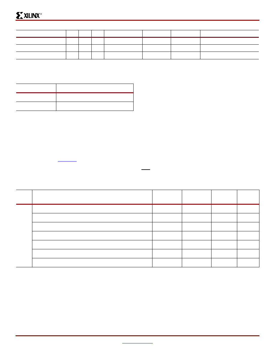
Table 8:
Configuration Codes
Configuration Mode
M2
M1
M0
CCLK Direction
Data Width
Serial Dout
Configuration Pull-ups
Table 9:
Virtex-E Bitstream Lengths
Device
# of Configuration Bits
XCV405E
3,430,400
XCV812E
6,519,648
Table 10:
Master/Slave Serial Mode Programming Switching
Description
Figure
References
Symbol
Values
Units
CCLK
DIN setup/hold, slave mode
1/2
TDCC/TCCD
5.0/0.0
ns, min
DIN setup/hold, master mode
1/2
TDSCK/TCKDS
5.0/0.0
ns, min
DOUT
3TCCO
12.0
ns, max
High time
4TCCH
5.0
ns, min
Low time
5TCCL
5.0
ns, min
Maximum Frequency
FCC
66
MHz, max
Frequency Tolerance, master mode with respect to nominal
+45% –30%
相关PDF资料 |
PDF描述 |
|---|---|
| XCV405E-6BG560I | IC FPGA 1.8V 560-MBGA |
| XC6VCX130T-2FFG484I | IC FPGA VIRTEX 6 128K 484FFGBGA |
| XCV600E-7FG900C | IC FPGA 1.8V C-TEMP 900-FBGA |
| XCV600E-6FG900I | IC FPGA 1.8V I-TEMP 900-FBGA |
| XC2V2000-5FG676I | IC FPGA VIRTEX-II 676FGBGA |
相关代理商/技术参数 |
参数描述 |
|---|---|
| XCV405E-7BG560I | 功能描述:IC FPGA 1.8V 560-MBGA RoHS:否 类别:集成电路 (IC) >> 嵌入式 - FPGA(现场可编程门阵列) 系列:Virtex®-E EM 产品变化通告:Step Intro and Pkg Change 11/March/2008 标准包装:1 系列:Virtex®-5 SXT LAB/CLB数:4080 逻辑元件/单元数:52224 RAM 位总计:4866048 输入/输出数:480 门数:- 电源电压:0.95 V ~ 1.05 V 安装类型:表面贴装 工作温度:-40°C ~ 100°C 封装/外壳:1136-BBGA,FCBGA 供应商设备封装:1136-FCBGA 配用:568-5088-ND - BOARD DEMO DAC1408D750122-1796-ND - EVALUATION PLATFORM VIRTEX-5 |
| XCV405E-7BG676C | 制造商:XILINX 制造商全称:XILINX 功能描述:Virtex-E 1.8 V Extended Memory Field Programmable Gate Arrays |
| XCV405E-7BG676I | 制造商:XILINX 制造商全称:XILINX 功能描述:Virtex-E 1.8 V Extended Memory Field Programmable Gate Arrays |
| XCV405E-7BG900C | 制造商:XILINX 制造商全称:XILINX 功能描述:Virtex-E 1.8 V Extended Memory Field Programmable Gate Arrays |
| XCV405E-7BG900I | 制造商:XILINX 制造商全称:XILINX 功能描述:Virtex-E 1.8 V Extended Memory Field Programmable Gate Arrays |
发布紧急采购,3分钟左右您将得到回复。