参数资料
| 型号: | XCV405E-7BG560C |
| 厂商: | Xilinx Inc |
| 文件页数: | 65/118页 |
| 文件大小: | 0K |
| 描述: | IC FPGA 1.8V C-TEMP 560-MBGA |
| 产品变化通告: | FPGA Family Discontinuation 18/Apr/2011 |
| 标准包装: | 1 |
| 系列: | Virtex®-E EM |
| LAB/CLB数: | 2400 |
| 逻辑元件/单元数: | 10800 |
| RAM 位总计: | 573440 |
| 输入/输出数: | 404 |
| 门数: | 129600 |
| 电源电压: | 1.71 V ~ 1.89 V |
| 安装类型: | 表面贴装 |
| 工作温度: | 0°C ~ 85°C |
| 封装/外壳: | 560-LBGA,金属 |
| 供应商设备封装: | 560-MBGA(42.5x42.5) |
第1页第2页第3页第4页第5页第6页第7页第8页第9页第10页第11页第12页第13页第14页第15页第16页第17页第18页第19页第20页第21页第22页第23页第24页第25页第26页第27页第28页第29页第30页第31页第32页第33页第34页第35页第36页第37页第38页第39页第40页第41页第42页第43页第44页第45页第46页第47页第48页第49页第50页第51页第52页第53页第54页第55页第56页第57页第58页第59页第60页第61页第62页第63页第64页当前第65页第66页第67页第68页第69页第70页第71页第72页第73页第74页第75页第76页第77页第78页第79页第80页第81页第82页第83页第84页第85页第86页第87页第88页第89页第90页第91页第92页第93页第94页第95页第96页第97页第98页第99页第100页第101页第102页第103页第104页第105页第106页第107页第108页第109页第110页第111页第112页第113页第114页第115页第116页第117页第118页
Virtex-E 1.8 V Extended Memory Field Programmable Gate Arrays
Module 2 of 4
DS025-2 (v3.0) March 21, 2014
46
R
— OBSOLETE — OBSOLETE — OBSOLETE — OBSOLETE —
Termination Resistor Packs
Resistor packs are available with the values and the config-
uration required for LVDS and LVPECL termination from
Bourns, Inc., as listed in Table. For pricing and availability,
please contact Bourns directly at www.bourns.com.
LVDS Design Guide
The SelectI/O library elements have been expanded for Vir-
tex-E devices to include new LVDS variants. At this time all
of the cells might not be included in the Synthesis libraries.
The 2.1i-Service Pack 2 update for Alliance and Foundation
software includes these cells in the VHDL and Verilog librar-
ies. It is necessary to combine these cells to create the
P-side (positive) and N-side (negative) as described in the
input, output, 3-state and bidirectional sections.
Creating LVDS Global Clock Input Buffers
The global clock input buffer can be combined with the adja-
cent IOB to form an LVDS clock input buffer. The P-side
resides in the GCLKPAD location and the N-side resides in
the adjacent IO_LVDS_DLL site.
HDL Instantiation
Only one global clock input buffer is required to be instanti-
ated in the design and placed on the correct GCLKPAD
location. The N-side of the buffer is reserved and no other
IOB is allowed to be placed on this location.
In the physical device, a configuration option is enabled that
routes the pad wire to the differential input buffer located in
the GCLKIOB. The output of this buffer then drives the out-
put of the GCLKIOB cell. In EPIC it appears that the second
buffer is unused. Any attempt to use this location for another
purpose leads to a DRC error in the software.
VHDL Instantiation
gclk0_p : IBUFG_LVDS port map
(I=>clk_external, O=>clk_internal);
Verilog Instantiation
IBUFG_LVDS gclk0_p (.I(clk_external),
.O(clk_internal));
Location Constraints
All LVDS buffers must be explicitly placed on a device. For
the global clock input buffers this can be done with the fol-
lowing constraint in the UCF or NCF file.
NET clk_external LOC = GCLKPAD3;
GCLKPAD3 can also be replaced with the package pin
name, such as D17 for the BG432 package.
Optional N-Side
Some designers might prefer to also instantiate the N-side
buffer for the global clock buffer. This allows the top-level net
list to include net connections for both PCB layout and sys-
tem-level integration. In this case, only the output P-side
IBUFG connection has a net connected to it. Since the
N-side IBUFG does not have a connection in the EDIF net
list, it is trimmed from the design in MAP.
VHDL Instantiation
gclk0_p : IBUFG_LVDS port map
(I=>clk_p_external, O=>clk_internal);
gclk0_n : IBUFG_LVDS port map
(I=>clk_n_external, O=>clk_internal);
Verilog Instantiation
IBUFG_LVDS gclk0_p (.I(clk_p_external),
.O(clk_internal));
IBUFG_LVDS gclk0_n (.I(clk_n_external),
.O(clk_internal));
Location Constraints
All LVDS buffers must be explicitly placed on a device. For
the global clock input buffers this can be done with the fol-
lowing constraint in the UCF or NCF file.
NET clk_p_external LOC = GCLKPAD3;
NET clk_n_external LOC = C17;
Table 40:
Bourns LVDS/LVPECL Resistor Packs
Part Number
I/O Standard
Term.
for:
Pairs/
Pack
Pins
CAT16
LV2F6
LVDS
Driver
2
8
CAT16
LV4F12
LVDS
Driver
4
16
CAT16
PC2F6
LVPECL
Driver
2
8
CAT16
PC4F12
LVPECL
Driver
4
16
CAT16
PT2F2
LVDS/LVPECL
Receiver
2
8
CAT16
PT4F4
LVDS/LVPECL
Receiver
4
16
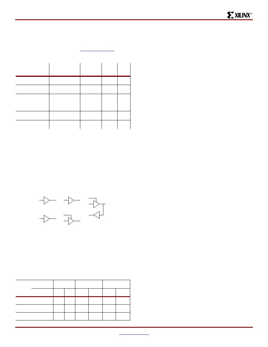
Figure 58: LVDS Elements
Table 41:
Global Clock Input Buffer Pair Locations
Pkg
Pair 3
Pair 2
Pair 0
PN
P
N
P
N
P
N
BG560
A17
C18
D17
E17
AJ17
AM18
AL17
AM17
FG676
E13
B13
C13
F14
AB13
AF13
AA14
AC14
FG900
C15
A15
E15
E16
AK16
AH16
AJ16
AF16
O
I
IBUF_LVDS
O
I
OBUF_LVDS
IOBUF_LVDS
O
T
I
OBUFT_LVDS
O
I
IBUFG_LVDS
IO
T
I
x133_22_122299
相关PDF资料 |
PDF描述 |
|---|---|
| XCV405E-6BG560I | IC FPGA 1.8V 560-MBGA |
| XC6VCX130T-2FFG484I | IC FPGA VIRTEX 6 128K 484FFGBGA |
| XCV600E-7FG900C | IC FPGA 1.8V C-TEMP 900-FBGA |
| XCV600E-6FG900I | IC FPGA 1.8V I-TEMP 900-FBGA |
| XC2V2000-5FG676I | IC FPGA VIRTEX-II 676FGBGA |
相关代理商/技术参数 |
参数描述 |
|---|---|
| XCV405E-7BG560I | 功能描述:IC FPGA 1.8V 560-MBGA RoHS:否 类别:集成电路 (IC) >> 嵌入式 - FPGA(现场可编程门阵列) 系列:Virtex®-E EM 产品变化通告:Step Intro and Pkg Change 11/March/2008 标准包装:1 系列:Virtex®-5 SXT LAB/CLB数:4080 逻辑元件/单元数:52224 RAM 位总计:4866048 输入/输出数:480 门数:- 电源电压:0.95 V ~ 1.05 V 安装类型:表面贴装 工作温度:-40°C ~ 100°C 封装/外壳:1136-BBGA,FCBGA 供应商设备封装:1136-FCBGA 配用:568-5088-ND - BOARD DEMO DAC1408D750122-1796-ND - EVALUATION PLATFORM VIRTEX-5 |
| XCV405E-7BG676C | 制造商:XILINX 制造商全称:XILINX 功能描述:Virtex-E 1.8 V Extended Memory Field Programmable Gate Arrays |
| XCV405E-7BG676I | 制造商:XILINX 制造商全称:XILINX 功能描述:Virtex-E 1.8 V Extended Memory Field Programmable Gate Arrays |
| XCV405E-7BG900C | 制造商:XILINX 制造商全称:XILINX 功能描述:Virtex-E 1.8 V Extended Memory Field Programmable Gate Arrays |
| XCV405E-7BG900I | 制造商:XILINX 制造商全称:XILINX 功能描述:Virtex-E 1.8 V Extended Memory Field Programmable Gate Arrays |
发布紧急采购,3分钟左右您将得到回复。