参数资料
| 型号: | XCV812E-8FG900C |
| 厂商: | Xilinx Inc |
| 文件页数: | 92/118页 |
| 文件大小: | 0K |
| 描述: | IC FPGA 1.8V C-TEMP 900-FBGA |
| 产品变化通告: | FPGA Family Discontinuation 18/Apr/2011 |
| 标准包装: | 1 |
| 系列: | Virtex®-E EM |
| LAB/CLB数: | 4704 |
| 逻辑元件/单元数: | 21168 |
| RAM 位总计: | 1146880 |
| 输入/输出数: | 556 |
| 门数: | 254016 |
| 电源电压: | 1.71 V ~ 1.89 V |
| 安装类型: | 表面贴装 |
| 工作温度: | 0°C ~ 85°C |
| 封装/外壳: | 900-BBGA |
| 供应商设备封装: | 900-FBGA |
第1页第2页第3页第4页第5页第6页第7页第8页第9页第10页第11页第12页第13页第14页第15页第16页第17页第18页第19页第20页第21页第22页第23页第24页第25页第26页第27页第28页第29页第30页第31页第32页第33页第34页第35页第36页第37页第38页第39页第40页第41页第42页第43页第44页第45页第46页第47页第48页第49页第50页第51页第52页第53页第54页第55页第56页第57页第58页第59页第60页第61页第62页第63页第64页第65页第66页第67页第68页第69页第70页第71页第72页第73页第74页第75页第76页第77页第78页第79页第80页第81页第82页第83页第84页第85页第86页第87页第88页第89页第90页第91页当前第92页第93页第94页第95页第96页第97页第98页第99页第100页第101页第102页第103页第104页第105页第106页第107页第108页第109页第110页第111页第112页第113页第114页第115页第116页第117页第118页
Virtex-E 1.8 V Extended Memory Field Programmable Gate Arrays
DS025-3 (v3.0) March 21, 2014
Module 3 of 4
19
R
— OBSOLETE — OBSOLETE — OBSOLETE — OBSOLETE —
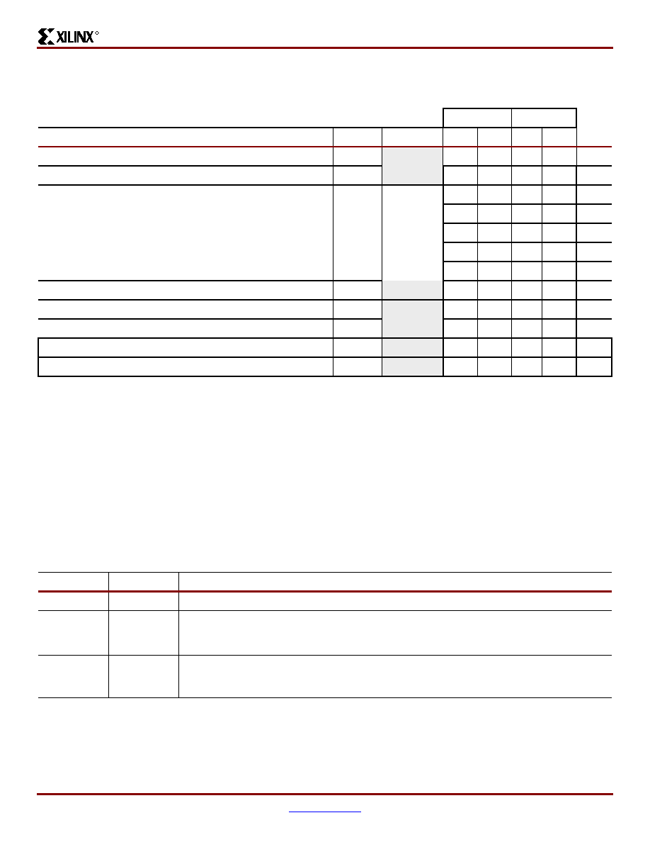
DLL Clock Tolerance, Jitter, and Phase Information
All DLL output jitter and phase specifications determined through statistical measurement at the package pins using a clock
mirror configuration and matched drivers.
Revision History
The following table shows the revision history for this document.
CLKDLLHF
CLKDLL
Units
Description
Symbol
F
CLKIN
Min
Max
Min
Max
Input Clock Period Tolerance
TIPTOL
-1.0
-
1.0
ns
Input Clock Jitter Tolerance (Cycle to Cycle)
TIJITCC
-
± 150
-
± 300
ps
Time Required for DLL to Acquire Lock(6)
TLOCK
> 60 MHz
-
20
-
20
μs
50 - 60 MHz
-
25
μs
40 - 50 MHz
-
50
μs
30 - 40 MHz
-
90
μs
25 - 30 MHz
-
120
μs
Output Jitter (cycle-to-cycle) for any DLL Clock Output(1)
TOJITCC
± 60
ps
Phase Offset between CLKIN and CLKO(2)
TPHIO
± 100
ps
Phase Offset between Clock Outputs on the DLL(3)
TPHOO
± 140
ps
Maximum Phase Difference between CLKIN and CLKO(4)
TPHIOM
± 160
ps
Maximum Phase Difference between Clock Outputs on the DLL(5)
TPHOOM
± 200
ps
Notes:
1.
Output Jitter is cycle-to-cycle jitter measured on the DLL output clock and is based on a maximum tap delay resolution, excluding
input clock jitter.
2.
Phase Offset between CLKIN and CLKO is the worst-case fixed time difference between rising edges of CLKIN and CLKO,
excluding Output Jitter and input clock jitter.
3.
Phase Offset between Clock Outputs on the DLL is the worst-case fixed time difference between rising edges of any two DLL
outputs, excluding Output Jitter and input clock jitter.
4.
Maximum Phase Difference between CLKIN an CLKO is the sum of Output Jitter and Phase Offset between CLKIN and CLKO,
or the greatest difference between CLKIN and CLKO rising edges due to DLL alone (excluding input clock jitter).
5.
Maximum Phase DIfference between Clock Outputs on the DLL is the sum of Output JItter and Phase Offset between any DLL
clock outputs, or the greatest difference between any two DLL output rising edges sue to DLL alone (excluding input clock jitter).
6.
Add 30% to the value for Industrial grade parts.
Date
Version
Revision
03/23/2000
1.0
Initial Xilinx release.
08/01/2000
1.1
Accumulated edits and fixes. Upgrade to Preliminary. Preview -8 numbers added.
Reformatted to adhere to corporate documentation style guidelines. Minor changes in
BG560 pin-out table.
09/19/2000
1.2
In Table 3 (Module 4), FG676 Fine-Pitch BGA — XCV405E, the following pins are no
longer labeled as VREF: B7, G16, G26, W26, AF20, AF8, Y1, H1.
Min values added to Virtex-E Electrical Characteristics tables.
相关PDF资料 |
PDF描述 |
|---|---|
| XE8801AMI000WP | SENSING MACHINE WITH 16 + 10 BIT |
| XE8802MI035LF | IC DAS 16BIT FLASH 8K 100-LQFP |
| XE8805AMI028LF | IC DAS 16BIT FLASH 8K MTP 64LQFP |
| XE8807AMI026TLF | IC MCU LOW PWR MTP FLASH 32-TQFP |
| XIO2200AGGW | IC PCI-EXPRESS/BUS BRIDGE 176BGA |
相关代理商/技术参数 |
参数描述 |
|---|---|
| XCV812E-8FG900I | 制造商:XILINX 制造商全称:XILINX 功能描述:Virtex-E 1.8 V Extended Memory Field Programmable Gate Arrays |
| XCVR-040L31 | 制造商:WWP 功能描述: |
| XCW 10 | 制造商:G & J HALL 功能描述:COUNTERSINK HEXIBIT 10MM 制造商:G & J HALL 功能描述:COUNTERSINK, HEXIBIT, 10MM 制造商:G & J HALL 功能描述:COUNTERSINK, HEXIBIT, 10MM; Drill Bit Size Metric:10mm; Overall Length:30.5mm; SVHC:No SVHC (19-Dec-2012); Countersink Angle:90; Drill Bit Type:Countersink; Drill Point Diameter:10mm; External Diameter:10mm; Head Diameter:10mm; ;RoHS Compliant: NA |
| XCW10 | 制造商:G & J HALL 功能描述:COUNTERSINK HEXIBIT |
| XCW15 | 制造商:G & J HALL 功能描述:COUNTERSINK HEXIBIT |
发布紧急采购,3分钟左右您将得到回复。