- 您现在的位置:买卖IC网 > PDF目录4039 > XPC8260ZUIHBC (Freescale Semiconductor)IC MPU POWERQUICC II 480-TBGA PDF资料下载
参数资料
| 型号: | XPC8260ZUIHBC |
| 厂商: | Freescale Semiconductor |
| 文件页数: | 3/41页 |
| 文件大小: | 0K |
| 描述: | IC MPU POWERQUICC II 480-TBGA |
| 标准包装: | 21 |
| 系列: | MPC82xx |
| 处理器类型: | 32-位 MPC82xx PowerQUICC II |
| 速度: | 200MHz |
| 电压: | 2.5V |
| 安装类型: | 表面贴装 |
| 封装/外壳: | 480-LBGA |
| 供应商设备封装: | 408-TBGA(37.5x37.5) |
| 包装: | 托盘 |
第1页第2页当前第3页第4页第5页第6页第7页第8页第9页第10页第11页第12页第13页第14页第15页第16页第17页第18页第19页第20页第21页第22页第23页第24页第25页第26页第27页第28页第29页第30页第31页第32页第33页第34页第35页第36页第37页第38页第39页第40页第41页
MPC8260 PowerQUICC II Integrated Communications Processor Hardware Specifications, Rev. 2
Freescale Semiconductor
11
Electrical and Thermal Characteristics
2.3.1
Layout Practices
Each VCC pin should be provided with a low-impedance path to the board’s power supply. Each ground
pin should likewise be provided with a low-impedance path to ground. The power supply pins drive
distinct groups of logic on chip. The VCC power supply should be bypassed to ground using at least four
0.1 F by-pass capacitors located as close as possible to the four sides of the package. The capacitor leads
and associated printed circuit traces connecting to chip VCC and ground should be kept to less than half an
inch per capacitor lead. A four-layer board is recommended, employing two inner layers as V
CC and GND
planes.
All output pins on the MPC8260 have fast rise and fall times. Printed circuit (PC) trace interconnection
length should be minimized in order to minimize overdamped conditions and reflections caused by these
fast output switching times. This recommendation particularly applies to the address and data buses.
Maximum PC trace lengths of six inches are recommended. Capacitance calculations should consider all
device loads as well as parasitic capacitances due to the PC traces. Attention to proper PCB layout and
bypassing becomes especially critical in systems with higher capacitive loads because these loads create
higher transient currents in the VCC and GND circuits. Pull up all unused inputs or signals that will be
inputs during reset. Special care should be taken to minimize the noise levels on the PLL supply pins.
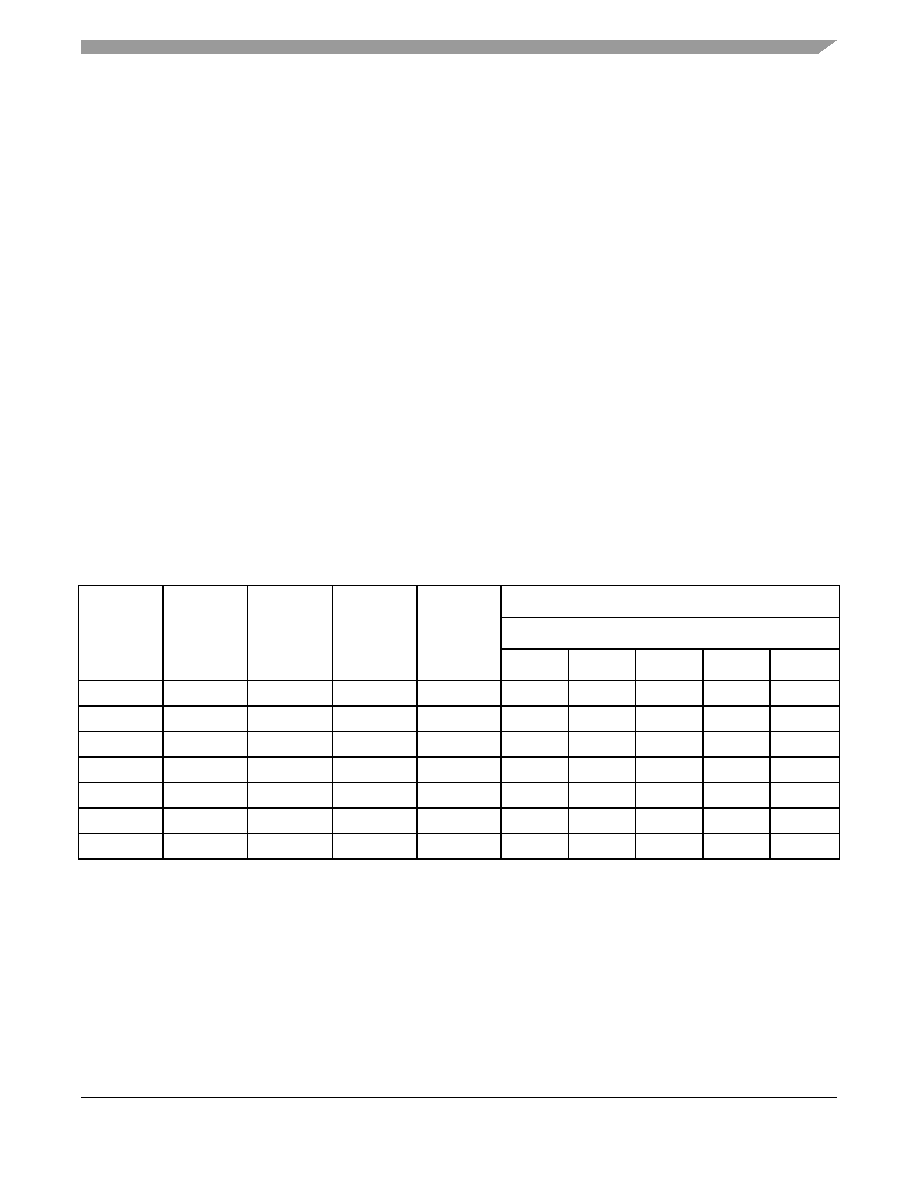
Table 5 provides preliminary, estimated power dissipation for various configurations. Note that suitable
thermal management is required for conditions above PD = 3W (when the ambient temperature is 70° C or
greater) to ensure the junction temperature does not exceed the maximum specified value. Also note that
the I/O power should be included when determining whether to use a heat sink.
Table 5. Estimated Power Dissipation for Various Configurations1
1 Test temperature = room temperature (25° C)
Bus
(MHz)
CPM
Multiplier
CPU
Multiplier
CPM
(MHz)
CPU
(MHz)
PINT (W)
2
2 P
INT = IDD x VDD Watts
Vddl
2.4
2.5
2.6
2.7
2.83
3 2.8 Vddl does not apply to HiP3 Rev C silicon.
33.3
4
133.3
2.04
2.14
2.26
2.38
2.50
50.0
2
3
100
150.0
2.21
2.30
2.45
2.59
2.69
66.7
2
2.5
133.3
166.7
2.47
2.62
2.74
2.88
3.02
66.7
2.5
166.7
2.57
2.69
2.83
2.98
3.12
66.7
2
3
133.3
200.0
2.81
2.95
3.12
3.29
3.43
66.7
2.5
3
166.7
200.0
2.88
3.05
3.22
3.38
3.55
50.0
3
4
150
200.0
2.83
3.00
3.14
3.31
3.48
Note:
相关PDF资料 |
PDF描述 |
|---|---|
| IDT70P248L55BYGI | IC SRAM 64KBIT 55NS 108PGA |
| XPC8260CZUIFBC | IC MPU POWERQUICC II 480-TBGA |
| IDT70P247L55BYGI | IC SRAM 64KBIT 55NS 100BGA |
| 65801-135LF | CLINCHER RECEPTACLE ASSY GOLD |
| 65801-035LF | CLINCHER RECEPTACLE ASS'-Y-GOLD |
相关代理商/技术参数 |
参数描述 |
|---|---|
| XPC8315E-RDB | 制造商:Freescale Semiconductor 功能描述: |
| XPC850CVR50BU | 功能描述:IC MPU POWERQUICC 50MHZ 256-PBGA RoHS:是 类别:集成电路 (IC) >> 嵌入式 - 微处理器 系列:MPC8xx 标准包装:2 系列:MPC8xx 处理器类型:32-位 MPC8xx PowerQUICC 特点:- 速度:133MHz 电压:3.3V 安装类型:表面贴装 封装/外壳:357-BBGA 供应商设备封装:357-PBGA(25x25) 包装:托盘 |
| XPC850CVR50BUR2 | 功能描述:IC MPU POWERQUICC 50MHZ 256-PBGA RoHS:是 类别:集成电路 (IC) >> 嵌入式 - 微处理器 系列:MPC8xx 标准包装:2 系列:MPC8xx 处理器类型:32-位 MPC8xx PowerQUICC 特点:- 速度:133MHz 电压:3.3V 安装类型:表面贴装 封装/外壳:357-BBGA 供应商设备封装:357-PBGA(25x25) 包装:托盘 |
| XPC850CVR66BU | 功能描述:IC MPU POWERQUICC 66MHZ 256-PBGA RoHS:是 类别:集成电路 (IC) >> 嵌入式 - 微处理器 系列:MPC8xx 标准包装:2 系列:MPC8xx 处理器类型:32-位 MPC8xx PowerQUICC 特点:- 速度:133MHz 电压:3.3V 安装类型:表面贴装 封装/外壳:357-BBGA 供应商设备封装:357-PBGA(25x25) 包装:托盘 |
| XPC850CZT50B | 制造商:MOTOROLA 制造商全称:Motorola, Inc 功能描述:Communications Controller Hardware Specifications |
发布紧急采购,3分钟左右您将得到回复。