参数资料
| 型号: | XRT72L53IB-F |
| 厂商: | Exar Corporation |
| 文件页数: | 414/467页 |
| 文件大小: | 0K |
| 描述: | IC FRAMER DS3/E3 3CH 272PBGA |
| 产品变化通告: | XRT72Lx Series Obsolescence 02/May/2012 |
| 标准包装: | 40 |
| 控制器类型: | DS3/E3 调帧器 |
| 电源电压: | 3.3V |
| 电流 - 电源: | 190mA |
| 工作温度: | -40°C ~ 85°C |
| 安装类型: | 表面贴装 |
| 封装/外壳: | 272-BBGA |
| 供应商设备封装: | 272-PBGA(27x27) |
| 包装: | 托盘 |
第1页第2页第3页第4页第5页第6页第7页第8页第9页第10页第11页第12页第13页第14页第15页第16页第17页第18页第19页第20页第21页第22页第23页第24页第25页第26页第27页第28页第29页第30页第31页第32页第33页第34页第35页第36页第37页第38页第39页第40页第41页第42页第43页第44页第45页第46页第47页第48页第49页第50页第51页第52页第53页第54页第55页第56页第57页第58页第59页第60页第61页第62页第63页第64页第65页第66页第67页第68页第69页第70页第71页第72页第73页第74页第75页第76页第77页第78页第79页第80页第81页第82页第83页第84页第85页第86页第87页第88页第89页第90页第91页第92页第93页第94页第95页第96页第97页第98页第99页第100页第101页第102页第103页第104页第105页第106页第107页第108页第109页第110页第111页第112页第113页第114页第115页第116页第117页第118页第119页第120页第121页第122页第123页第124页第125页第126页第127页第128页第129页第130页第131页第132页第133页第134页第135页第136页第137页第138页第139页第140页第141页第142页第143页第144页第145页第146页第147页第148页第149页第150页第151页第152页第153页第154页第155页第156页第157页第158页第159页第160页第161页第162页第163页第164页第165页第166页第167页第168页第169页第170页第171页第172页第173页第174页第175页第176页第177页第178页第179页第180页第181页第182页第183页第184页第185页第186页第187页第188页第189页第190页第191页第192页第193页第194页第195页第196页第197页第198页第199页第200页第201页第202页第203页第204页第205页第206页第207页第208页第209页第210页第211页第212页第213页第214页第215页第216页第217页第218页第219页第220页第221页第222页第223页第224页第225页第226页第227页第228页第229页第230页第231页第232页第233页第234页第235页第236页第237页第238页第239页第240页第241页第242页第243页第244页第245页第246页第247页第248页第249页第250页第251页第252页第253页第254页第255页第256页第257页第258页第259页第260页第261页第262页第263页第264页第265页第266页第267页第268页第269页第270页第271页第272页第273页第274页第275页第276页第277页第278页第279页第280页第281页第282页第283页第284页第285页第286页第287页第288页第289页第290页第291页第292页第293页第294页第295页第296页第297页第298页第299页第300页第301页第302页第303页第304页第305页第306页第307页第308页第309页第310页第311页第312页第313页第314页第315页第316页第317页第318页第319页第320页第321页第322页第323页第324页第325页第326页第327页第328页第329页第330页第331页第332页第333页第334页第335页第336页第337页第338页第339页第340页第341页第342页第343页第344页第345页第346页第347页第348页第349页第350页第351页第352页第353页第354页第355页第356页第357页第358页第359页第360页第361页第362页第363页第364页第365页第366页第367页第368页第369页第370页第371页第372页第373页第374页第375页第376页第377页第378页第379页第380页第381页第382页第383页第384页第385页第386页第387页第388页第389页第390页第391页第392页第393页第394页第395页第396页第397页第398页第399页第400页第401页第402页第403页第404页第405页第406页第407页第408页第409页第410页第411页第412页第413页当前第414页第415页第416页第417页第418页第419页第420页第421页第422页第423页第424页第425页第426页第427页第428页第429页第430页第431页第432页第433页第434页第435页第436页第437页第438页第439页第440页第441页第442页第443页第444页第445页第446页第447页第448页第449页第450页第451页第452页第453页第454页第455页第456页第457页第458页第459页第460页第461页第462页第463页第464页第465页第466页第467页
á
á THREE CHANNEL DS3/E3 FRAMER IC WITH HDLC CONTROLLER XRT72L53
PRELIMINARY
REV. P1.1.7
50
2.0
THE MICROPROCESSOR INTERFACE
BLOCK
The Microprocessor Interface section supports com-
munication between the local microprocessor (P)
and the Framer IC. In particular, the Microprocessor
Interface section supports the following operations
between the local microprocessor and the Framer.
Channel Selection
The writing of configuration data into the Framer
on-chip (addressable) registers.
The writing of an outbound PMDL (Path Mainte-
nance Data Link) message into the Transmit LAPD
Message buffer (within the Framer IC).
The Framer IC's generation of an Interrupt Request
to the P.
The P's servicing of the interrupt request from the
Framer IC.
The monitoring of the system's health by periodi-
cally reading the on-chip Performance Monitor reg-
isters.
The reading of an inbound PMDL Message from
the Receive LAPD Message Buffer (within the
Framer IC).
Each of these operations (between the local micro-
processor and the Framer IC) will be discussed in
some detail, throughout this data sheet.
2.1
CHANNEL SELECTION WITHIN THE XRT72L53
The XRT72L53 3-Channel DS3/E3 Clear Channel
Framer IC consists of three independent banks of
Configuration registers. Each of these banks are
identical and correspond to each of the three chan-
nels within the XRT72L53. The XRT72L53 is used to
select and access any one of these Configuration
Register Banks, via the two (2) Most Significant Ad-
dress Pins, A9 and A10.
The relationship between the states of A9 and A10,
and the corresponding Configuration Register bank,
is tabulated below.
The remaining Address Bus pins [A8 through A0] are
used to select the individual configuration registers
(within the selected configuration register bank) for
Read/Write access.
Looking at this Another Way
Each of the three (3) Configuration Register Banks,
within the XRT72L53 DS3/E3 Framer IC has an iden-
tical set of configuration registers. However, address
pins A9 and A10 impose the following address loca-
tion offset, for each of the Configuration Register
Bank within the address space of the XRT72L53.
Figure 24 presents a simple block diagram of the Mi-
croprocessor Interface Section, within the Framer IC.
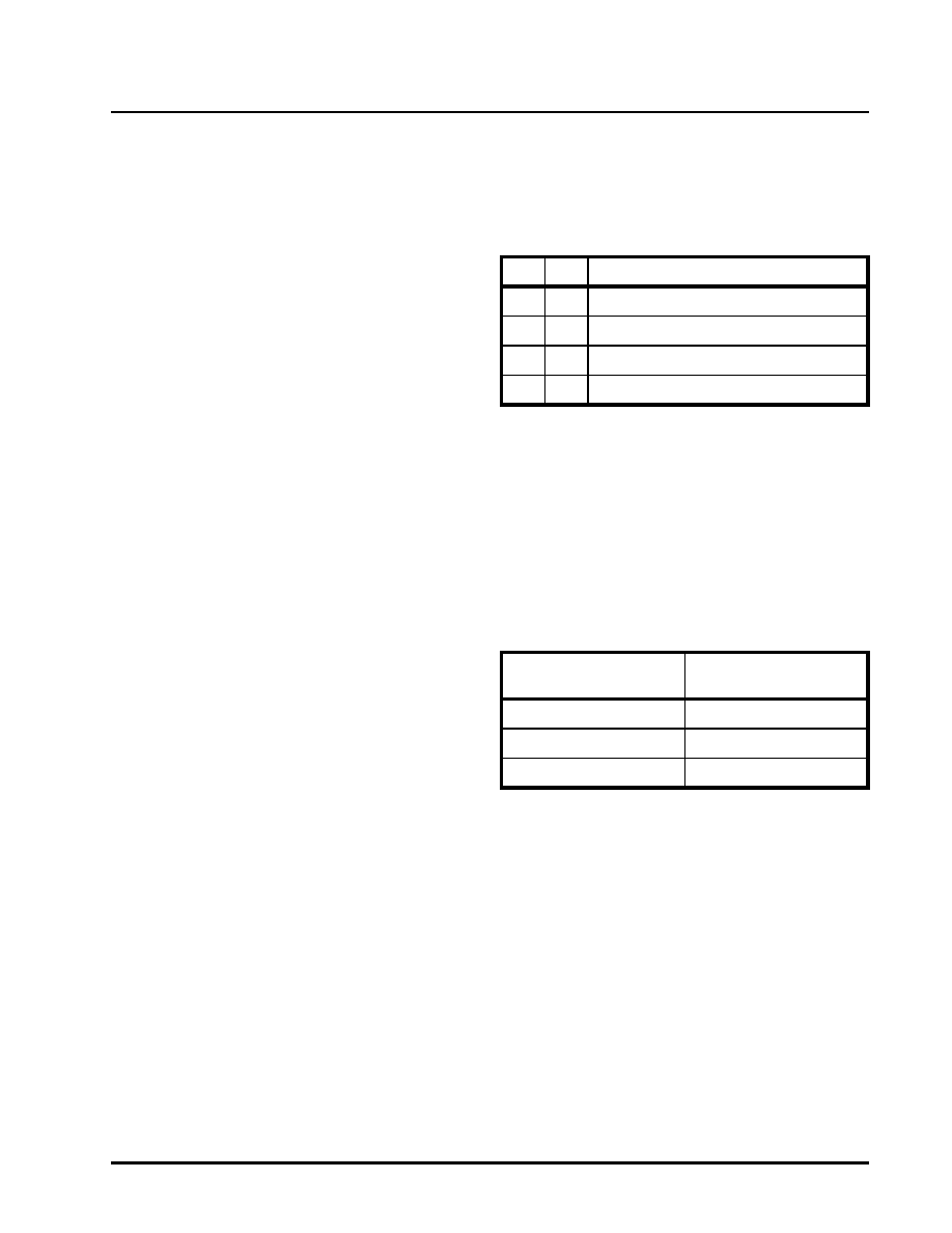
TABLE 1: THE RELATIONSHIP BETWEEN ADDRESS BITS
A9, A10 AND THE SELECTED CONFIGURATION
REGISTER BANK
A10
A9
CONFIGURATION REGISTER BANK SELECTED
0
Channel 0
0
1
Channel 1
1
0
Channel 2
11
Not Valid
CONFIGURATION REGISTER
BANK - CHANNEL NUMBER
ADDRESS OFFSET (WITHIN THE
XRT72L53 ADDRESS SPACE)
00x000
10x200
20x400
相关PDF资料 |
PDF描述 |
|---|---|
| XRT72L54IB | IC FRAMER DS3/E3 4CH 272PBGA |
| XRT72L71IQ | IC FRAMER DS3 ATM UNI 160PQFP |
| XRT73L02MIV-F | IC LIU E3/DS3/STS-1 2CH 100TQFP |
| XRT73L03BIV-F | IC LIU E3/DS3/STS-1 3CH 120LQFP |
| XRT73L04BIV-F | IC LIU E3/DS3/STS-1 4CH 144LQFP |
相关代理商/技术参数 |
参数描述 |
|---|---|
| XRT72L54 | 制造商:EXAR 制造商全称:EXAR 功能描述:FOUR CHANNEL DS3/E3 FRAMER IC WITH HDLC CONTROLLER |
| XRT72L54ES-PCI | 功能描述:网络控制器与处理器 IC with T73LC04A+T71D04 RoHS:否 制造商:Micrel 产品:Controller Area Network (CAN) 收发器数量: 数据速率: 电源电流(最大值):595 mA 最大工作温度:+ 85 C 安装风格:SMD/SMT 封装 / 箱体:PBGA-400 封装:Tray |
| XRT72L54IB | 功能描述:网络控制器与处理器 IC RoHS:否 制造商:Micrel 产品:Controller Area Network (CAN) 收发器数量: 数据速率: 电源电流(最大值):595 mA 最大工作温度:+ 85 C 安装风格:SMD/SMT 封装 / 箱体:PBGA-400 封装:Tray |
| XRT72L56 | 制造商:EXAR 制造商全称:EXAR 功能描述:SIX CHANNEL DS3/E3 FRAMER IC WITH HDLC CONTROLLER |
| XRT72L56ES-PCI | 功能描述:网络控制器与处理器 IC RoHS:否 制造商:Micrel 产品:Controller Area Network (CAN) 收发器数量: 数据速率: 电源电流(最大值):595 mA 最大工作温度:+ 85 C 安装风格:SMD/SMT 封装 / 箱体:PBGA-400 封装:Tray |
发布紧急采购,3分钟左右您将得到回复。