参数资料
| 型号: | XRT83L30IV-F |
| 厂商: | Exar Corporation |
| 文件页数: | 40/78页 |
| 文件大小: | 0K |
| 描述: | IC LIU LH/SH T1/E1 SGL 64TQFP |
| 标准包装: | 160 |
| 类型: | 线路接口装置(LIU) |
| 驱动器/接收器数: | 1/1 |
| 规程: | T1,E1 |
| 电源电压: | 3.135 V ~ 3.465 V |
| 安装类型: | 表面贴装 |
| 封装/外壳: | 64-LQFP |
| 供应商设备封装: | 64-TQFP(10x10) |
| 包装: | 托盘 |
| 其它名称: | 1016-1633 XRT83L30IV-F-ND |
第1页第2页第3页第4页第5页第6页第7页第8页第9页第10页第11页第12页第13页第14页第15页第16页第17页第18页第19页第20页第21页第22页第23页第24页第25页第26页第27页第28页第29页第30页第31页第32页第33页第34页第35页第36页第37页第38页第39页当前第40页第41页第42页第43页第44页第45页第46页第47页第48页第49页第50页第51页第52页第53页第54页第55页第56页第57页第58页第59页第60页第61页第62页第63页第64页第65页第66页第67页第68页第69页第70页第71页第72页第73页第74页第75页第76页第77页第78页
XRT83L30
42
REV. 1.0.1
SINGLE-CHANNEL T1/E1/J1 LH/SH TRANSCEIVER WITH CLOCK RECOVERY AND JITTER ATTENUATOR
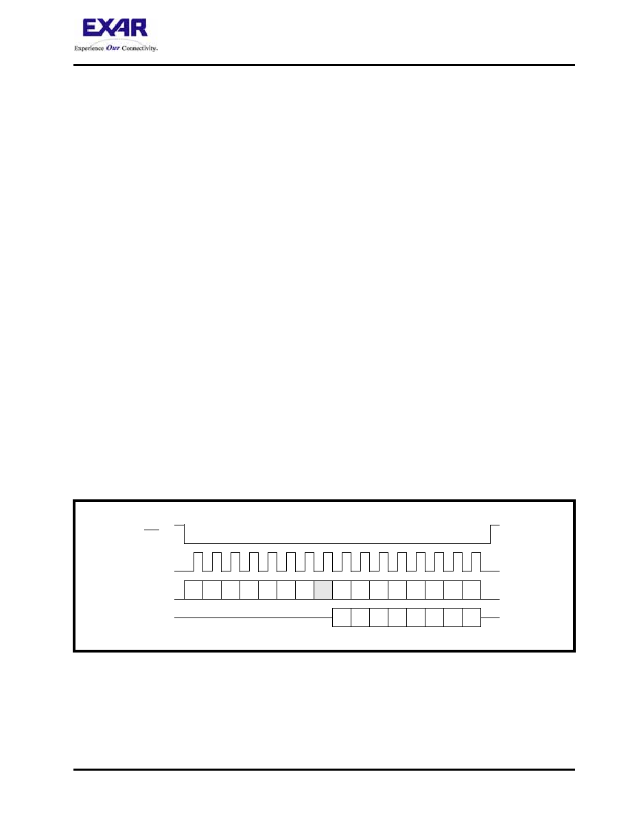
Bit 2 through 6:The five (5) Address Values (labeled A0, A1, A2, A3 and A4)
The next five rising edges of the SCLK signal, clock in the 5-bit address value for the Read or Write operation.
These five bits define the register address within XRT83L30 that the user has selected to read data from or
write data to. The address bits must be supplied to the SDI input in ascending order with LSB (Least Significant
Bit) first.
Bit 7:
(A5)
The next bit A5 must be set to “0” as shown in Figure 25.
Bit 8:
(A6)
The value of A6 is a “don’t care”.
Once the first eight bits have been written into the Serial interface, the subsequent action depends on the
whether the current operation is a “Read” or “Write” instruction.
Read Operation
With the last address bit “A4” written into the SDI input, the “Read” operation will proceed through an idle
period lasting two SCLK periods. On the rising edge of the 9th SCLK the serial data output (SDO) becomes
active (see Figure 25). At this point the user can begin reading the 8-bit data (D0 through D7) stored in the
interface register at address [A4,A3,A2,A1,A0], in ascending order (LSB first), on the falling edge of SCLK.
Write Operation
With the last address bit (A4) written into the SDI input, the “Write” operation will proceed through an idle
period lasting two SCLK periods. Prior to the rising edge of the 9th SCLK, the user must begin to apply the
eight bit data word to the SDI input. The Serial Interface will latch this data on the rising edge of SCLK. The
serial data (D0 through D7) should enter the SDI input in ascending order with the LSB first.
Serial Interface Register Description
The serial Interface consists of 32 8-bit register locations. The Microprocessor register address map and Bit
map are described in Table 16 and Table 17 respectively. The function of the individual bits are described in
FIGURE 25. MICROPROCESSOR SERIAL INTERFACE DATA STRUCTURE
5
6
7
8
1
2
3
4
13
14
15
16
9
10
11
12
R/W
Ao
A1
A2
A3
A4
0
A6
D0
D1
D2
D3
D4
D5
D6
D7
D0
D1
D2
D3
D4
D5
D6
D7
CS
SCLK
SDI
SDO
High Z
相关PDF资料 |
PDF描述 |
|---|---|
| XRT83L314IB-L | IC LIU T1/E1/J1 14CH 304TBGA |
| XRT83L34IV-F | IC LIU T1/E1/J1 QUAD 128TQFP |
| XRT83L38IB-F | IC LIU T1/E1/J1 OCTAL 225BGA |
| XRT83SH314IB-F | IC LIU T1/E1/J1 14CH 304TBGA |
| XRT83SH38IB-F | IC LIU SH T1/E1/J1 8CH 225BGA |
相关代理商/技术参数 |
参数描述 |
|---|---|
| XRT83L314 | 制造商:EXAR 制造商全称:EXAR 功能描述:14-CHANNEL T1/E1/J1 LONG-HAUL/SHORT-HAUL LINE INTERFACE UNIT |
| XRT83L314ES | 功能描述:LIN 收发器 RoHS:否 制造商:NXP Semiconductors 工作电源电压: 电源电流: 最大工作温度: 封装 / 箱体:SO-8 |
| XRT83L314IB | 功能描述:时钟合成器/抖动清除器 RoHS:否 制造商:Skyworks Solutions, Inc. 输出端数量: 输出电平: 最大输出频率: 输入电平: 最大输入频率:6.1 GHz 电源电压-最大:3.3 V 电源电压-最小:2.7 V 封装 / 箱体:TSSOP-28 封装:Reel |
| XRT83L314IB-F | 功能描述:时钟合成器/抖动清除器 RoHS:否 制造商:Skyworks Solutions, Inc. 输出端数量: 输出电平: 最大输出频率: 输入电平: 最大输入频率:6.1 GHz 电源电压-最大:3.3 V 电源电压-最小:2.7 V 封装 / 箱体:TSSOP-28 封装:Reel |
| XRT83L314IB-L | 功能描述:LIN 收发器 14 channel, LH/SH T1/E1 LIU RoHS:否 制造商:NXP Semiconductors 工作电源电压: 电源电流: 最大工作温度: 封装 / 箱体:SO-8 |
发布紧急采购,3分钟左右您将得到回复。