参数资料
| 型号: | XRT91L31IQ-F |
| 厂商: | Exar Corporation |
| 文件页数: | 3/41页 |
| 文件大小: | 0K |
| 描述: | IC TXRX SONET/SDH 8BIT 64QFP |
| 标准包装: | 1 |
| 类型: | 收发器,多路复用器 |
| PLL: | 是 |
| 主要目的: | 以太网,SONET/SDH |
| 输入: | LVCMOS,LVPECL,LVTTL |
| 输出: | LVCMOS,LVPECL,LVTTL |
| 电路数: | 1 |
| 差分 - 输入:输出: | 是/是 |
| 频率 - 最大: | 622.08MHz |
| 电源电压: | 3.135 V ~ 3.465 V |
| 工作温度: | -40°C ~ 85°C |
| 安装类型: | 表面贴装 |
| 封装/外壳: | 64-FQFP |
| 供应商设备封装: | 64-PQFP(10x10) |
| 包装: | 托盘 |
| 其它名称: | 1016-1361 |
第1页第2页当前第3页第4页第5页第6页第7页第8页第9页第10页第11页第12页第13页第14页第15页第16页第17页第18页第19页第20页第21页第22页第23页第24页第25页第26页第27页第28页第29页第30页第31页第32页第33页第34页第35页第36页第37页第38页第39页第40页第41页
XRT91L31
11
REV. 1.0.2
STS-12/STM-4 OR STS-3/STM-1 SONET/SDH TRANSCEIVER
RECEIVER SECTION
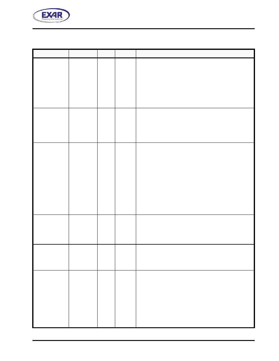
PIN DESCRIPTION
NAME
LEVEL
TYPE
PIN
DESCRIPTION
RXDO0
RXDO1
RXDO2
RXDO3
RXDO4
RXDO5
RXDO6
RXDO7
LVTTL,
LVCMOS
O
19
20
22
23
24
25
26
27
Receive Parallel Data Output
77.76 Mbps (STS-12/STM-4) / 19.44 Mbps (STS-3/STM-1)
8-bit parallel receive data output is updated simultaneously on
the falling edge of the RXPCLKO output. The 8-bit parallel
interface is de-multiplexed from the receive serial data input
MSB first (RXDO[7]). The XRT91L31 will output the data on the
falling edge of RXPCLKO clock.
RXIP
RXIN
Diff LVPECL
I
13
14
Receive Serial Data Input
The differential receive serial data stream of 622.08 Mbps
STS-12/STM-1 or 155.52 Mbps STS-3/STM-1 is applied to
these input pins. These pins have internal LVPECL common-
mode biasing circuit. External 100R termination is required
between RXIP/N pins.
XRXCLKIP
XRXCLKIN
Diff LVPECL
I
8
9
External Recovered Receive Clock Input
The differential receive serial data stream of 622.08 Mbps
STS-12/STM-1 or 155.52 Mbps STS-3/STM-1 is sampled on
the rising edge of this externally recovered differential clock
coming from the optical module. It is used when the internal
CDR unit is disabled and bypassed by the CDRDIS pin.
These pins have internal LVPECL common-mode biasing cir-
cuit. External 100R termination is required between XRX-
CLKIP/N pins.
NOTE: In the event that XRXCLKIP/N differential input pins are
unused, XRXCLKIP should be tied to VCC with a 1k
Ohm pull-up and XRXCLKIN should be tied to Ground
with a 1k Ohm pull-down.
RXPCLKO
LVTTL,
LVCMOS
O
29
Receive Parallel Clock Output (77.76 MHz or 19.44 MHz)
77.76 MHz (STS-12/STM-4) or 19.44 MHz (STS-3/STM-1)
clock output reference for the 8-bit parallel receive data output
RXDO[7:0]. The parallel received data output bus will be
updated on the falling edge of this clock.
CDRAUX-
REFCLK
LVTTL,
LVCMOS
I
32
Clock and Data Recovery Auxillary Reference Clock
77.76 MHz ± 200 ppm auxillary reference clock for the CDR.
NOTE: In the event that CDRAUXREFCLK LVTTL input pin is
unused, CDRAUXREFCLK should be tied to ground.
OOF
LVTTL,
LVCMOS
I
11
Out of Frame Input Indicator
This level sensitive input pin is used to initiate frame detection
and byte alignment recovery when OOF is declared by the
downstream device. When this pin is held High, FRAME-
PULSE will pulse for a single RXPCLKO period upon the detec-
tion of every third frame alignment A2 byte in the incoming
SONET/SDH Frame.
"Low" = Normal Operation
"High" = OOF Indication initiating frame detection and byte
boundary recovery and activating FRAMEPULSE
相关PDF资料 |
PDF描述 |
|---|---|
| MS27496E19A32S | CONN RCPT 32POS BOX MNT W/SCKT |
| AD9548BCPZ | IC CLOCK GEN/SYNCHRONIZR 88LFCSP |
| V375C36M150BL3 | CONVERTER MOD DC/DC 36V 150W |
| MAX3676EHJ+ | IC CLOCK RECOVERY 32-TQFP |
| ADN2813ACPZ | IC CLK/DATA REC 1.25GBPS 48LFCSP |
相关代理商/技术参数 |
参数描述 |
|---|---|
| XRT91L31IQ-F | 制造商:Exar Corporation 功能描述:SONET Transceiver IC |
| XRT91L31IQTR | 功能描述:总线收发器 SONET/SDH, FULL DPLX 3.3V I/O, LOS, CMU RoHS:否 制造商:Fairchild Semiconductor 逻辑类型:CMOS 逻辑系列:74VCX 每芯片的通道数量:16 输入电平:CMOS 输出电平:CMOS 输出类型:3-State 高电平输出电流:- 24 mA 低电平输出电流:24 mA 传播延迟时间:6.2 ns 电源电压-最大:2.7 V, 3.6 V 电源电压-最小:1.65 V, 2.3 V 最大工作温度:+ 85 C 封装 / 箱体:TSSOP-48 封装:Reel |
| XRT91L31IQTR-F | 功能描述:总线收发器 SONET/SDH, FULL DPLX 3.3V I/O, LOS, CMU RoHS:否 制造商:Fairchild Semiconductor 逻辑类型:CMOS 逻辑系列:74VCX 每芯片的通道数量:16 输入电平:CMOS 输出电平:CMOS 输出类型:3-State 高电平输出电流:- 24 mA 低电平输出电流:24 mA 传播延迟时间:6.2 ns 电源电压-最大:2.7 V, 3.6 V 电源电压-最小:1.65 V, 2.3 V 最大工作温度:+ 85 C 封装 / 箱体:TSSOP-48 封装:Reel |
| XRT91L32 | 制造商:EXAR 制造商全称:EXAR 功能描述:STS-12/STM-4 OR STS-3/STM-1 SONET/SDH TRANSCEIVER |
| XRT91L32ES | 功能描述:LIN 收发器 SONET SDH 8 bit TRANCEIVER RoHS:否 制造商:NXP Semiconductors 工作电源电压: 电源电流: 最大工作温度: 封装 / 箱体:SO-8 |
发布紧急采购,3分钟左右您将得到回复。