参数资料
| 型号: | XRT94L43IB-F |
| 厂商: | Exar Corporation |
| 文件页数: | 58/328页 |
| 文件大小: | 0K |
| 描述: | IC MAPPER SONET/SDH OC12 516BGA |
| 标准包装: | 24 |
| 应用: | 网络切换 |
| 接口: | 总线 |
| 电源电压: | 2.5V, 3.3V |
| 封装/外壳: | 516-BBGA |
| 供应商设备封装: | 516-PBGA(35x35) |
| 包装: | 托盘 |
| 安装类型: | 表面贴装 |
第1页第2页第3页第4页第5页第6页第7页第8页第9页第10页第11页第12页第13页第14页第15页第16页第17页第18页第19页第20页第21页第22页第23页第24页第25页第26页第27页第28页第29页第30页第31页第32页第33页第34页第35页第36页第37页第38页第39页第40页第41页第42页第43页第44页第45页第46页第47页第48页第49页第50页第51页第52页第53页第54页第55页第56页第57页当前第58页第59页第60页第61页第62页第63页第64页第65页第66页第67页第68页第69页第70页第71页第72页第73页第74页第75页第76页第77页第78页第79页第80页第81页第82页第83页第84页第85页第86页第87页第88页第89页第90页第91页第92页第93页第94页第95页第96页第97页第98页第99页第100页第101页第102页第103页第104页第105页第106页第107页第108页第109页第110页第111页第112页第113页第114页第115页第116页第117页第118页第119页第120页第121页第122页第123页第124页第125页第126页第127页第128页第129页第130页第131页第132页第133页第134页第135页第136页第137页第138页第139页第140页第141页第142页第143页第144页第145页第146页第147页第148页第149页第150页第151页第152页第153页第154页第155页第156页第157页第158页第159页第160页第161页第162页第163页第164页第165页第166页第167页第168页第169页第170页第171页第172页第173页第174页第175页第176页第177页第178页第179页第180页第181页第182页第183页第184页第185页第186页第187页第188页第189页第190页第191页第192页第193页第194页第195页第196页第197页第198页第199页第200页第201页第202页第203页第204页第205页第206页第207页第208页第209页第210页第211页第212页第213页第214页第215页第216页第217页第218页第219页第220页第221页第222页第223页第224页第225页第226页第227页第228页第229页第230页第231页第232页第233页第234页第235页第236页第237页第238页第239页第240页第241页第242页第243页第244页第245页第246页第247页第248页第249页第250页第251页第252页第253页第254页第255页第256页第257页第258页第259页第260页第261页第262页第263页第264页第265页第266页第267页第268页第269页第270页第271页第272页第273页第274页第275页第276页第277页第278页第279页第280页第281页第282页第283页第284页第285页第286页第287页第288页第289页第290页第291页第292页第293页第294页第295页第296页第297页第298页第299页第300页第301页第302页第303页第304页第305页第306页第307页第308页第309页第310页第311页第312页第313页第314页第315页第316页第317页第318页第319页第320页第321页第322页第323页第324页第325页第326页第327页第328页
XRT94L43
144
REV. 1.0.2
SONET/SDH OC-12 TO 12XDS3/E3 MAPPER
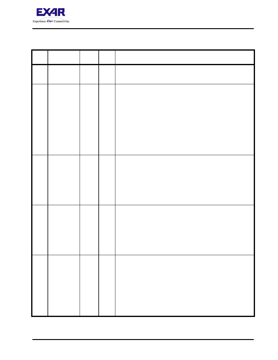
PIN DESCRIPTIONS - INDIRECT ADDRESSING
MICROPROCESSOR INTERFACE
PIN #
SIGNAL NAME
I/O
SIGNAL
TYPE
DESCRIPTION
U22
PCLK
I
TTL
Microprocessor Interface Clock Input:
This clock input signal is used for synchronous/burst/DMA data transfer
operations. This clock can be running up to 66MHz.
L25
L23
L22
PTYPE_0
PTYPE_1
PTYPE_2
I
TTL
Microprocessor Type Select input:
These three input pins are used to configure the Microprocessor Interface
block to readily support a wide variety of Microprocessor Interfaces. The
relationship between the settings of these input pins and the corresponding
Microprocessor Interface configuration is presented below.
PTYPE[2:0]
Microprocessor Interface Mode
000
Asynchronous Intel
l001
Asynchronous Motorola
010
Intel X86
011
Intel I960, Motorola MPC860
100
IDT3051/52 (MIPS)
101
IBM Power PC
V26
R24
P26
M24
T26
M22
M25
L26
PADDR_0
PADDR_1
PADDR_2
PADDR_3
PADDR_4
PADDR_5
PADDR_6
PADDR_7
I
TTL
Address Bus Input pins (Microprocessor Interface):
These pins are used to select the on-chip Mapper/Framer registers and
RAM space for READ and WRITE Operations with the Microprocessor.
T22
R22
U24
R21
W26
T25
R25
R26
PDATA_0
PDATA_1
PDATA_2
PDATA_3
PDATA_4
PDATA_5
PDATA_6
PDATA_7
I/O
TTL
Bi-Directional Data Bus Pins (Microprocessor Interface):
These pins are used to drive and receive data over the bi-directional data
bus.
Y26
PWR_L
I
TTL
Write Strobe (Intel Mode):
If the Microprocessor Interface is configured to operate in the Intel Mode,
then this active-low input pin functions as the WR (WRITE Strobe) input sig-
nal from the Microprocessor. Once this active-low signal is asserted, the
Mapper/Framer will latch the contents of the bi-directional data (D[7:0]) into
the addressed registers (or Buffer location) within the Mapper/Framer.
R/W Input Pin (Motorola Mode):
When the Microprocessor Interface Section is operating in the Motorola
Mode, then this pin is functionally equivalent to the R/W pin. In the Motorola
Mode, a READ operation occurs if this pin is at a logic 1. Similarly a WRITE
operation occurs if this pin is at a logic 0.
相关PDF资料 |
PDF描述 |
|---|---|
| XS1-G02B-FB144-I4 | IC MCU 32BIT 16KB OTP 144FBGA |
| XTR114U/2K5 | IC 4-20MA I-TRANSMITTER 14-SOIC |
| ZXHF5000JB24TC | IC SWITCH QUAD 2X1 24QFN |
| 3341-56 | IC PLL INTEGER-N 3GHZ 20QFN |
| 3342-56 | IC PLL INTEGER-N 3GHZ 20QFN |
相关代理商/技术参数 |
参数描述 |
|---|---|
| XRT94L55 | 制造商:EXAR 制造商全称:EXAR 功能描述:SONET/SDH OC-48/STM-16, 4XOC-12/STM-4, 16XOC-3/STM-1 FRAMER/CONCENTRATOR WITH INTEGRATED CDR’S |
| XRT94L55IV | 制造商:EXAR 制造商全称:EXAR 功能描述:SONET/SDH OC-48/STM-16, 4XOC-12/STM-4, 16XOC-3/STM-1 FRAMER/CONCENTRATOR WITH INTEGRATED CDR’S |
| XRT95L34 | 制造商:EXAR 制造商全称:EXAR 功能描述:OC-12/STM-4, QUAD OC-3/STM-1 POS/ATM FRAMER WITH INTEGRATED CDR’S |
| XRT95L34IV | 制造商:EXAR 制造商全称:EXAR 功能描述:OC-12/STM-4, QUAD OC-3/STM-1 POS/ATM FRAMER WITH INTEGRATED CDR’S |
| XRT95L51 | 制造商:EXAR 制造商全称:EXAR 功能描述:OC-48 ATM UNI/POS/MAPPER IC |
发布紧急采购,3分钟左右您将得到回复。