- 您现在的位置:买卖IC网 > PDF目录300164 > ZL30402/QCC1 (ZARLINK SEMICONDUCTOR INC) ATM/SONET/SDH SUPPORT CIRCUIT, PQFP80 PDF资料下载
参数资料
| 型号: | ZL30402/QCC1 |
| 厂商: | ZARLINK SEMICONDUCTOR INC |
| 元件分类: | 数字传输电路 |
| 英文描述: | ATM/SONET/SDH SUPPORT CIRCUIT, PQFP80 |
| 封装: | 14 X 14 MM, 1.40 MM HEIGHT, MS-026BEC, LQFP-80 |
| 文件页数: | 43/44页 |
| 文件大小: | 472K |
| 代理商: | ZL30402/QCC1 |
第1页第2页第3页第4页第5页第6页第7页第8页第9页第10页第11页第12页第13页第14页第15页第16页第17页第18页第19页第20页第21页第22页第23页第24页第25页第26页第27页第28页第29页第30页第31页第32页第33页第34页第35页第36页第37页第38页第39页第40页第41页第42页当前第43页第44页
ZL30402
Data Sheet
8
Zarlink Semiconductor Inc.
20
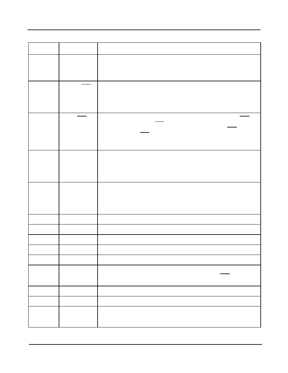
F8o
Frame Pulse ST-BUS/GCI 8.192 Mb/s (CMOS tristate output). This is an
8 kHz, 122 ns, active high framing pulse, which marks the beginning of a ST-
BUS/GCI frame. This is typically used for ST-BUS/GCI operation at
8.192 Mb/s. See Figure 13 for details.
21
E3DS3/OC3
E3DS3 or OC3 Selection (Input). In Hardware Control, a logic low on this pin
enables the C155P/N outputs (pin 30 and pin 31) and sets the C34/C44 output
(pin 53) to provide C8 or C11 clocks. Logic high at this input disables the C155
clock outputs (high impedance) and sets C34/C44 output to provide C34 and
C44 clocks. In Software Control connect this pin to ground.
22
E3/DS3
E3 or DS3 Selection (Input). In Hardware Control, when the E3DS3/OC3 pin
is set high, logic low on E3/DS3 pin selects a 44.736 MHz clock on C34/C44
output and logic high selects 34.368 MHz clock. When E3DS3/OC3 pin is set
low, logic low on E3/DS3 pin selects 11.184 MHz clock on C34/C44 output and
logic high selects 8.592 MHz clock. Connect this input to ground in Software
Control.
23
SEC
Secondary Reference (Input). This input is used as a secondary reference
source for synchronization. The ZL30402 can synchronize to the falling edge
of the 8 kHz, 1.544 MHz or 2.048 MHz clocks and the rising edge of the
19.44 MHz clock. In Hardware Control, selection of the input reference is
based upon the RefSel control input. This pin is internally pulled up to VDD.
24
PRI
Primary Reference (Input). This input is used as a primary reference source
for synchronization. The ZL30402 can synchronize to the falling edge of the
8 kHz, 1.544 MHz or 2.048 MHz clocks and the rising edge of the 19.44 MHz
clock. In Hardware Control, selection of the input reference is based upon the
RefSel control input. This pin is internally pulled up to VDD.
25
GND
Ground.
26
IC
Internal Connection. Leave unconnected.
27
GND
Ground.
28
AVDD
Positive Analog Power Supply. Connect this pin to VDD.
29
VDD
Positive Power Supply.
30
31
C155N
C155P
Clock 155.52 MHz (LVDS output). Differential outputs for a 155.52 MHz clock.
These outputs are enabled by applying logic low to E3DS3/OC3 input or they
can be switched into high impedance state by applying logic high.
32
GND
Ground.
33
NC
No internal bonding Connection. Leave unconnected.
34
Tdo
IEEE1149.1a Test Data Output (CMOS output). JTAG serial data is output on
this pin on the falling edge of Tclk clock. If not used, this pin should be left
unconnected.
Pin Description (continued)
Pin #
Name
Description
相关PDF资料 |
PDF描述 |
|---|---|
| ZL30402/QCG1 | ATM/SONET/SDH SUPPORT CIRCUIT, PQFP80 |
| ZL50112GAG2 | SPECIALTY TELECOM CIRCUIT, PBGA552 |
| ZL50112GAG | SPECIALTY TELECOM CIRCUIT, PBGA552 |
| ZL50114GAG2 | SPECIALTY TELECOM CIRCUIT, PBGA552 |
| ZL50114GAG | SPECIALTY TELECOM CIRCUIT, PBGA552 |
相关代理商/技术参数 |
参数描述 |
|---|---|
| ZL30402QCG1 | 制造商:Microsemi Corporation 功能描述:PB FREE SONET / SDH NETWORK ELEMENT PLL - Trays 制造商:MICROSEMI CONSUMER MEDICAL PRODUCT GROUP 功能描述:IC NETWORK PLL SONET/SDH 80LQFP 制造商:Microsemi Corporation 功能描述:IC NETWORK PLL SONET/SDH 80LQFP |
| ZL30406 | 制造商:ZARLINK 制造商全称:Zarlink Semiconductor Inc 功能描述:SONET/SDH Clock Multiplier PLL |
| ZL30406_06 | 制造商:ZARLINK 制造商全称:Zarlink Semiconductor Inc 功能描述:SONET/SDH Clock Multiplier PLL |
| ZL30406QGC | 制造商:Zarlink Semiconductor Inc 功能描述:PLL CLOCK MLTPLR SGL UP TO 19.44MHZ 64TQFP - Trays |
| ZL30406QGC1 | 制造商:ZARLINK 制造商全称:Zarlink Semiconductor Inc 功能描述:SONET/SDH Clock Multiplier PLL |
发布紧急采购,3分钟左右您将得到回复。