- 您现在的位置:买卖IC网 > PDF目录300164 > ZL50114GAG2 (XILINX INC) SPECIALTY TELECOM CIRCUIT, PBGA552 PDF资料下载
参数资料
| 型号: | ZL50114GAG2 |
| 厂商: | XILINX INC |
| 元件分类: | 通信及网络 |
| 英文描述: | SPECIALTY TELECOM CIRCUIT, PBGA552 |
| 封装: | 35 X 35 MM, 1.27 MM PITCH, LEAD FREE, PLASTIC, MS-034, BGA-552 |
| 文件页数: | 1/113页 |
| 文件大小: | 2004K |
| 代理商: | ZL50114GAG2 |
当前第1页第2页第3页第4页第5页第6页第7页第8页第9页第10页第11页第12页第13页第14页第15页第16页第17页第18页第19页第20页第21页第22页第23页第24页第25页第26页第27页第28页第29页第30页第31页第32页第33页第34页第35页第36页第37页第38页第39页第40页第41页第42页第43页第44页第45页第46页第47页第48页第49页第50页第51页第52页第53页第54页第55页第56页第57页第58页第59页第60页第61页第62页第63页第64页第65页第66页第67页第68页第69页第70页第71页第72页第73页第74页第75页第76页第77页第78页第79页第80页第81页第82页第83页第84页第85页第86页第87页第88页第89页第90页第91页第92页第93页第94页第95页第96页第97页第98页第99页第100页第101页第102页第103页第104页第105页第106页第107页第108页第109页第110页第111页第112页第113页
1
Zarlink Semiconductor Inc.
Zarlink, ZL and the Zarlink Semiconductor logo are trademarks of Zarlink Semiconductor Inc.
Copyright 2003-2009, Zarlink Semiconductor Inc. All Rights Reserved.
Features
General
Circuit Emulation Services over Packet (CESoP)
transport for MPLS, IP and Ethernet networks
On chip timing & synchronization recovery across
a packet network
Grooming capability for Nx64 Kbps trunking
Circuit Emulation Services
Supports ITU-T Recommendation Y.1413 and
Y.1453
Supports IETF RFC4553 and RFC5086
Supports MEF8 and MFA 8.0.0
Structured, synchronous CESoP with clock
recovery
Unstructured, asynchronous CESoP, with integral
per stream clock recovery
TDM Interfaces
Up to 32 T1/E1, 8 J2, or 2 T3/E3 ports
H.110, H-MVIP, ST-BUS backplanes
Up to 1024 bi-directional 64 Kbps channels
Direct connection to LIUs, framers, backplanes
Dual reference Stratum 4 and 4E DPLL for
synchronous operation
Network Interfaces
Up to 3 x 100 Mbps MII Fast Ethernet or Dual
Redundant 1000 Mbps GMII/TBI Ethernet
Interfaces
System Interfaces
Flexible 32 bit host CPU interface (Motorola
PowerQUICC compatible)
On-chip packet memory for self-contained
operation, with buffer depths of over 16 ms
Up to 8 Mbytes of off-chip packet memory,
supporting buffer depths of over 128 ms
March 2009
Ordering Information
ZL50110GAG
552 PBGA
Trays, Bake & Drypack
ZL50111GAG
552 PBGA
Trays, Bake & Drypack
ZL50112GAG
552 PBGA
Trays, Bake & Drypack
ZL50114GAG
552 PBGA
Trays, Bake & Drypack
ZL50110GAG2
552 PBGA** Trays, Bake & Drypack
ZL50111GAG2
552 PBGA** Trays, Bake & Drypack
ZL50112GAG2
552 PBGA** Trays, Bake & Drypack
ZL50114GAG2
552 PBGA** Trays, Bake & Drypack
**Pb Fee Tin Silver/Copper
-40°C to +85°C
ZL50110/11/12/14
128, 256, 512 and 1024 Channel CESoP
Processors
Data Sheet
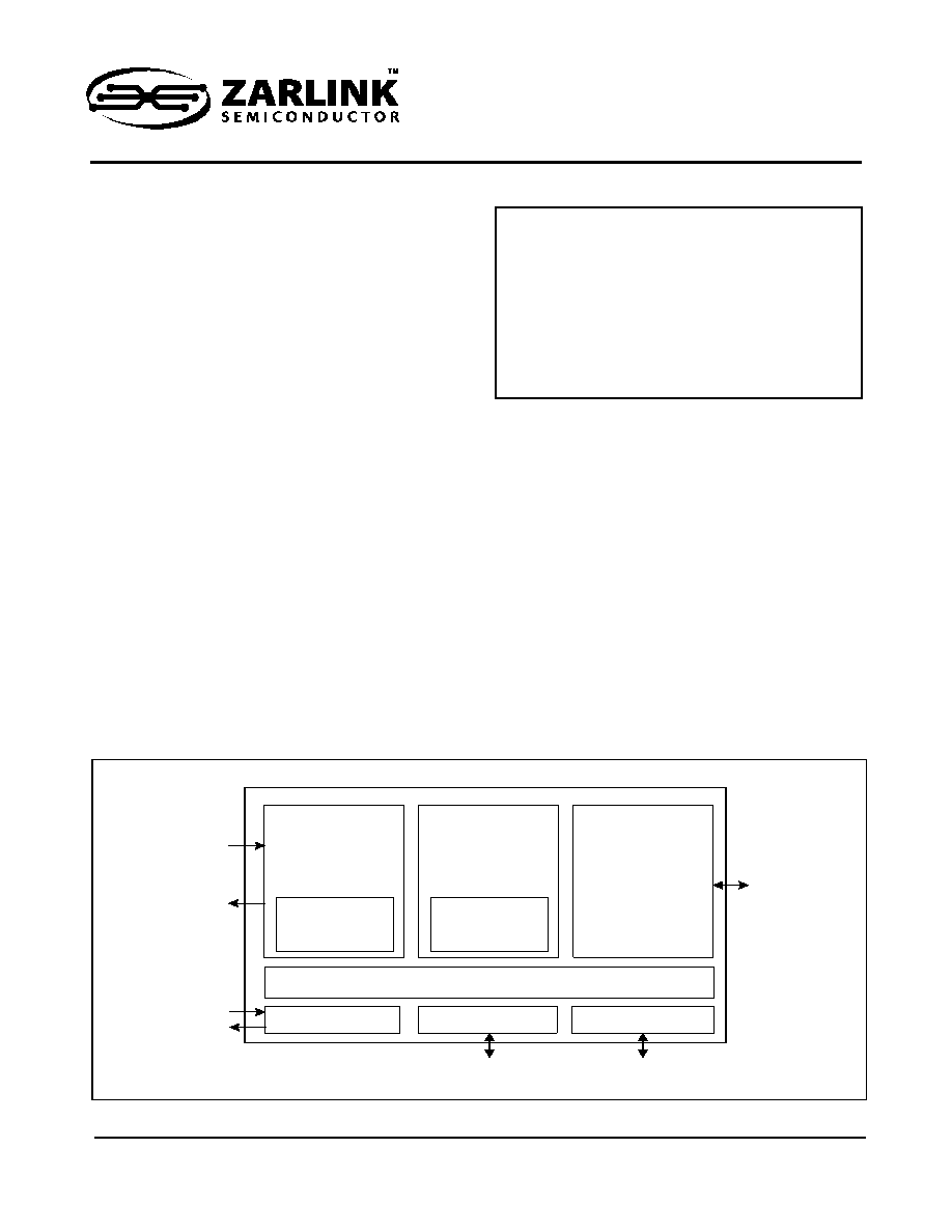
Figure 1 - ZL50111 High Level Overview
On C h ip P a c k e t Me m o ry
(J itte r B u ffe r C o m pens atio n fo r 16-128 m s of P a c k et D e la y V a riation)
D u al R e fe renc e
DP L L
H o st P ro c e sso r
In te rfa c e
E x te rn a l M e m o ry
In te rfac e (optio n a l)
H
.110
,
H
-M
VI
P,
ST
-B
U
S
bac
k
p
la
n
e
s
T
ri
p
le
1
0
M
bps
M
II
F
a
s
t
E
th
e
rne
t
or
D
u
a
l
R
e
dudn
at
1
000
M
b
p
s
G
M
II
/
TB
I
G
ig
a
b
it
Et
he
rn
e
t
B
a
c
k
p
lane
Cl
o
c
k
s
32-bit M o to ro la c o m p atib le P Q II
M u lti-P rotoc ol
P a cke t
P roc es s ing
En g in e
P W , RT P , UDP ,
IP v 4 , IP v 6 , M P L S ,
ECID , VL AN, U s e r
D e fined, O thers
Trip le
P a cke t
In te rfa c e
MA C
(M II, G M II, T B I)
TD M
In te rfa c e
(L IU , Fram er, B a c k pla ne)
Pe r Po rt DC O fo r
Clo c k Re c o v e ry
Z B T -SRAM
(0 - 8 M b y tes )
32
T
1
/E
1
,
8
J
2,
2
T
3/
E
3
p
o
rt
s
相关PDF资料 |
PDF描述 |
|---|---|
| ZL50114GAG | SPECIALTY TELECOM CIRCUIT, PBGA552 |
| ZL50232GD | DATACOM, ISDN ECHO CANCELLER, PBGA208 |
| ZL50233/GDG | DATACOM, ISDN ECHO CANCELLER, PBGA208 |
| ZL50408GDC | DATACOM, LAN SWITCHING CIRCUIT, PBGA208 |
| ZL50408GDG2 | DATACOM, LAN SWITCHING CIRCUIT, PBGA208 |
相关代理商/技术参数 |
参数描述 |
|---|---|
| ZL50115 | 制造商:ZARLINK 制造商全称:Zarlink Semiconductor Inc 功能描述:32, 64 and 128 Channel CESoP Processors |
| ZL50115GAG | 制造商:Microsemi Corporation 功能描述:SWIT FABRIC 1K X 1K 1.8V/3.3V 324BGA - Trays 制造商:Microsemi Corporation 功能描述:IC CESOP PROCESSOR 32CH 324PBGA |
| ZL50115GAG2 | 制造商:Microsemi Corporation 功能描述:PB FREE 1 TDM + 1 ETHERNET - Trays 制造商:Microsemi Corporation 功能描述:IC CESOP PROCESSOR 32CH 324PBGA |
| ZL50116 | 制造商:ZARLINK 制造商全称:Zarlink Semiconductor Inc 功能描述:32, 64 and 128 Channel CESoP Processors |
| ZL50116GAG | 制造商:Microsemi Corporation 功能描述:2 TDM + 1 ETHERNET - Trays 制造商:MICROSEMI CONSUMER MEDICAL PRODUCT GROUP 功能描述:IC CESOP PROCESSOR 64CH 324PBGA 制造商:Microsemi Corporation 功能描述:IC CESOP PROCESSOR 64CH 324PBGA |
发布紧急采购,3分钟左右您将得到回复。