- 您现在的位置:买卖IC网 > PDF目录222827 > 71V25781YSA166BGI (INTEGRATED DEVICE TECHNOLOGY INC) 256K X 18 CACHE SRAM, 3.5 ns, PBGA119 PDF资料下载
参数资料
| 型号: | 71V25781YSA166BGI |
| 厂商: | INTEGRATED DEVICE TECHNOLOGY INC |
| 元件分类: | SRAM |
| 英文描述: | 256K X 18 CACHE SRAM, 3.5 ns, PBGA119 |
| 封装: | BGA-119 |
| 文件页数: | 12/22页 |
| 文件大小: | 627K |
| 代理商: | 71V25781YSA166BGI |
6.42
2
IDT71V25761, IDT71V25781, 128K x 36, 256K x 18, 3.3V Synchronous SRAMs with
2.5V I/O, Pipelined Outputs, Burst Counter, Single Cycle Deselect
Commercial and Industrial Temperature Ranges
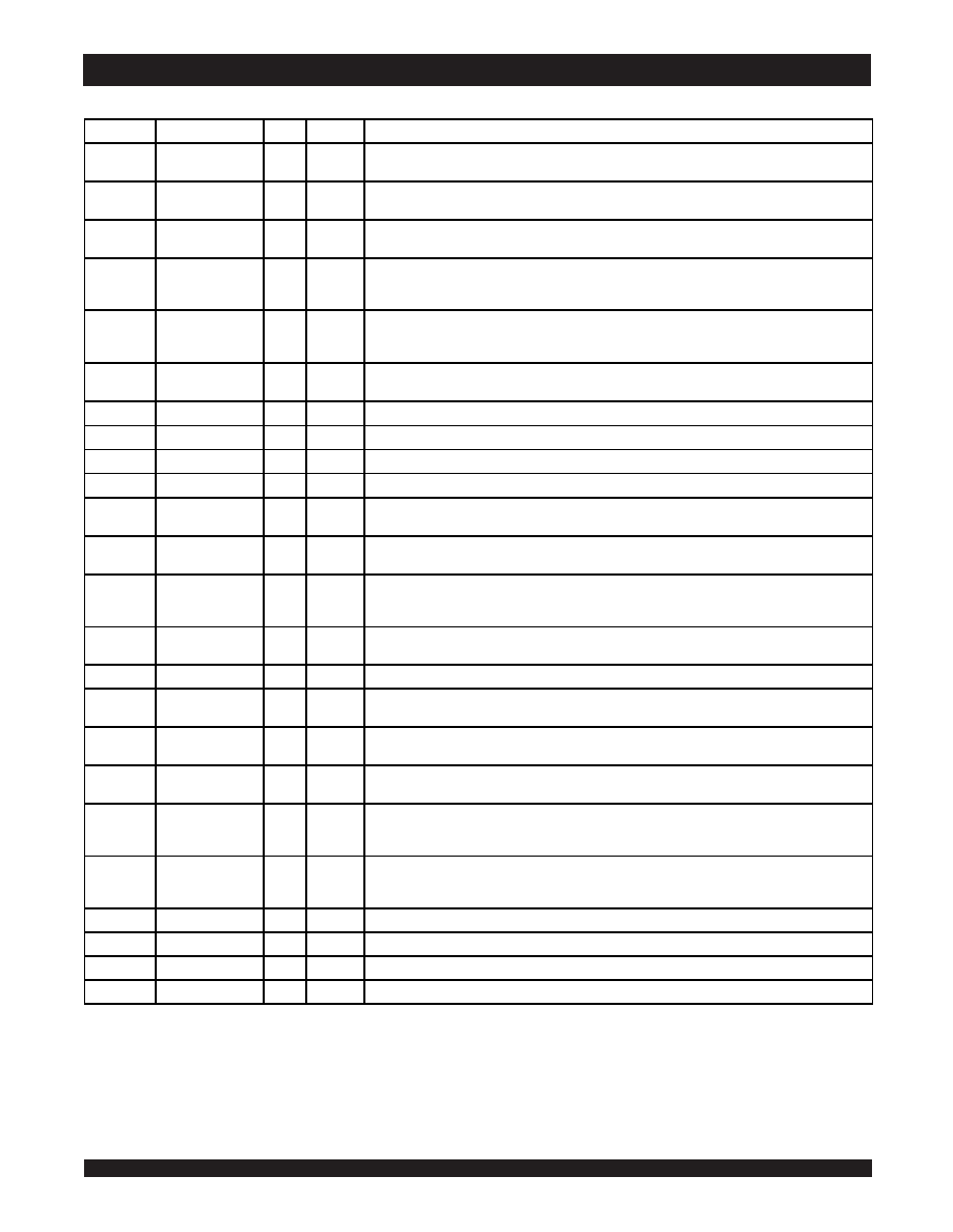
Symbol
Pin Function
I/O
Active
Description
A0-A17
Address Inputs
I
N/A
Synchronous Address inputs. The address register is triggered by a combination of the rising edge of CLK
and
ADSC Low or ADSP Low and CE Low.
ADSC
Address Status
(Cache Controller)
I
LOW
Synchronous Ad dress Status from Cache Controller.
ADSC is an active LOW input that is used to load the
address registers with new addresses.
ADSP
Address Status
(Processor)
I
LOW
Synchrono us Address Status from Processor.
ADSP is an active LOW input that is used to load the address
registers with new addresses.
ADSP is gated by CE.
ADV
Burst Address
Advance
I
LOW
Synchronous Address Advance.
ADV is an active LOW input that is used to advance the internal burst
counter, controlling burst access after the initial address is loaded. When the input is HIGH the burst counter is
not incremented; that is, there is no address advance.
BWE
Byte Write Enable
I
LOW
Synchronous byte write enable gates the byte write inputs
BW1-BW4. If BWE is LOW at the rising edge of CLK
then
BWx inputs are passed to the next stage in the circuit. If BWE is HIGH then the byte write inputs are
blocked and only
GW can initiate a write cycle.
BW1-BW4
Individual Byte
Write Enables
I
LOW
Synchronous byte write enables.
BW1 controls I/O0-7, I/OP1, BW2 controls I/O8-15, I/OP2, etc. Any active byte
write causes all outputs to be disabled.
CE
Chip Enable
I
LOW
Synchronous chip enable.
CE is used with CS0 and CS1 to enable the IDT71V25761/781. CE also gates ADSP.
CLK
Clock
I
N/A
This is the clock input. All timing references for the device are made with respect to this input.
CS0
Chip Select 0
I
HIGH
Synchronous active HIGH chip select. CS0 is used with
CE and CS1 to enable the chip.
CS1
Chip Select 1
I
LOW
Synchronous active LOW chip select.
CS1 is used with CE and CS0 to enable the chip.
GW
Global Write
Enable
I
LOW
Synchronous global write enable. This input will write all four 9-bit data bytes when LOW on the rising edge of
CLK.
GW supersedes individual byte write enables.
I/O0-I/O31
I/OP1-I/OP4
Data Input/Output
I/O
N/A
Synchronous data input/output (I/O) pins. Both the data input path and data output path are registered and
triggered by the rising edge of CLK.
LBO
Linear Burst Order
I
LOW
Asynchronous burst order selection input. When
LBO is HIGH, the interleaved burst sequence is selected.
When
LBO is LOW the Linear burst sequence is selected. LBO is a static input and must not change state
while the device is operating.
OE
Output Enable
I
LOW
Asynchronous output enable. When
OE is LOW the data output drivers are enabled on the I/O pins if the chip
is also selected. When
OE is HIGH the I/O pins are in a high-impedance state.
TMS
Test ModeSelect
I
N/A
Gives input command for TAP controller. Sampled on rising edge of TDK. This pin has an internal pullup.
TDI
Test Data Input
I
N/A
Serial input of registers placed between TDI and TDO. Sampled on rising edge of TCK. This pin has an
internal pullup.
TCK
Test Clock
I
N/A
Clock input of TAP controller. Each TAP event is clocked. Test inputs are captured o n rising edge of TCK,
while test outputs are d riven from the falling edge of TCK. This pin has an internal pullup.
TDO
Test DataOutput
O
N/A
Serial output of registers placed between TDI and TDO. This output is active depending on the state of the
TAP controller.
TRST
JTAG Reset
(Optional)
ILOW
Optional Asynchronous JTAG reset. Can be used to reset the TAP co ntroller, but not required. JTAG reset
occurs automatically at power up and also resets using TMS and TCK per IEEE 1149.1. If not used
TRST can
be left floating. This pin has an internal pullup. Only available in BGA package.
ZZ
Sleep Mode
I
HIGH
Asynchronous sleep mode input. ZZ HIGH will gate the CLK internally and power down the IDT71V25761/781
to its lowest power consumption level. Data retention is guaranteed in Sleep Mode.This pin has an internal
pull down.
VDD
Power Supply
N/A
3.3V core power supply.
VDDQ
Power Supply
N/A
2.5V I/O Supply.
VSS
Ground
N/A
Ground.
NC
No Connect
N/A
NC pins are not electrically connected to the device.
5297 tbl 02
Pin Definitions(1)
NOTE:
1. All synchronous inputs must meet specified setup and hold times with respect to CLK.
相关PDF资料 |
PDF描述 |
|---|---|
| 71V35761YSA183BGI8 | 128K X 36 CACHE SRAM, 3.3 ns, PBGA119 |
| 71V35781S183PF | 256K X 18 CACHE SRAM, 3.3 ns, PQFP100 |
| 7201LA20JGI | 512 X 9 OTHER FIFO, 20 ns, PQCC32 |
| 72031-111LF | 36 CONTACT(S), MALE, STRAIGHT TWO PART BOARD CONNECTOR, PRESS FIT |
| 72031-111 | 36 CONTACT(S), MALE, STRAIGHT TWO PART BOARD CONNECTOR, PRESS FIT |
相关代理商/技术参数 |
参数描述 |
|---|---|
| 71V30L25TF | 功能描述:静态随机存取存储器 1Kx8 ASYNCHRONOUS 3.3V DUAL-PORT RAM RoHS:否 制造商:Cypress Semiconductor 存储容量:16 Mbit 组织:1 M x 16 访问时间:55 ns 电源电压-最大:3.6 V 电源电压-最小:2.2 V 最大工作电流:22 uA 最大工作温度:+ 85 C 最小工作温度:- 40 C 安装风格:SMD/SMT 封装 / 箱体:TSOP-48 封装:Tray |
| 71V30L25TF8 | 功能描述:静态随机存取存储器 1Kx8 ASYNCHRONOUS 3.3V DUAL-PORT RAM RoHS:否 制造商:Cypress Semiconductor 存储容量:16 Mbit 组织:1 M x 16 访问时间:55 ns 电源电压-最大:3.6 V 电源电压-最小:2.2 V 最大工作电流:22 uA 最大工作温度:+ 85 C 最小工作温度:- 40 C 安装风格:SMD/SMT 封装 / 箱体:TSOP-48 封装:Tray |
| 71V30L25TFG | 功能描述:静态随机存取存储器 1Kx8 ASYNCHRONOUS 3.3V DUAL-PORT RAM RoHS:否 制造商:Cypress Semiconductor 存储容量:16 Mbit 组织:1 M x 16 访问时间:55 ns 电源电压-最大:3.6 V 电源电压-最小:2.2 V 最大工作电流:22 uA 最大工作温度:+ 85 C 最小工作温度:- 40 C 安装风格:SMD/SMT 封装 / 箱体:TSOP-48 封装:Tray |
| 71V30L25TFG8 | 功能描述:静态随机存取存储器 1Kx8 ASYNCHRONOUS 3.3V DUAL-PORT RAM RoHS:否 制造商:Cypress Semiconductor 存储容量:16 Mbit 组织:1 M x 16 访问时间:55 ns 电源电压-最大:3.6 V 电源电压-最小:2.2 V 最大工作电流:22 uA 最大工作温度:+ 85 C 最小工作温度:- 40 C 安装风格:SMD/SMT 封装 / 箱体:TSOP-48 封装:Tray |
| 71V30L25TFGI | 制造商:Integrated Device Technology Inc 功能描述:1KX8 LOW POWER 8K 3.3V DUAL PORT RAM - Bulk |
发布紧急采购,3分钟左右您将得到回复。