参数资料
| 型号: | AD5735ACPZ |
| 厂商: | Analog Devices Inc |
| 文件页数: | 25/48页 |
| 文件大小: | 0K |
| 描述: | IC DAC QUAD VOLT CUR 64-LFCSP |
| 标准包装: | 1 |
| 设置时间: | 18µs |
| 位数: | 12 |
| 数据接口: | DSP,MICROWIRE?,QSPI?,串行,SPI? |
| 转换器数目: | 4 |
| 电压电源: | 模拟和数字,双 ± |
| 工作温度: | -40°C ~ 105°C |
| 安装类型: | 表面贴装 |
| 封装/外壳: | 64-VFQFN 裸露焊盘,CSP |
| 供应商设备封装: | 64-LFCSP-VQ(9x9) |
| 包装: | 托盘 |
| 输出数目和类型: | 4 电流,4 电压 |
| 采样率(每秒): | * |
第1页第2页第3页第4页第5页第6页第7页第8页第9页第10页第11页第12页第13页第14页第15页第16页第17页第18页第19页第20页第21页第22页第23页第24页当前第25页第26页第27页第28页第29页第30页第31页第32页第33页第34页第35页第36页第37页第38页第39页第40页第41页第42页第43页第44页第45页第46页第47页第48页
Data Sheet
AD5735
Rev. C | Page 31 of 48
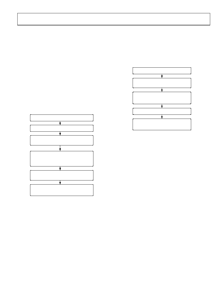
ENABLING THE OUTPUT
To correctly write to and set up the part from a power-on
condition, use the following sequence:
1. Perform a hardware or software reset after initial power-on.
2. Configure the dc-to-dc converter supply block. Set the
dc-to-dc switching frequency, the maximum output voltage
allowed, and the dc-to-dc converter phase between channels.
3. Configure the DAC control register on a per-channel basis.
Select the output range, and enable the dc-to-dc converter
block (DC_DC bit). Other control bits can also be config-
ured. Set the INT_ENABLE bit, but do not set the OUTEN
(output enable) bit.
4. Write the required code to the DAC data register. This step
implements a full internal DAC calibration. For reduced
output glitch, allow at least 200 s before performing Step 5.
5. Write to the DAC control register again to enable the
output (set the OUTEN bit).
Figure 73 provides a flowchart of this sequence.
POWER ON.
STEP 1: PERFORM A SOFTWARE/HARDWARE RESET.
STEP 4:
STEP 2: WRITE TO DC-TO-DC CONTROL REGISTER TO
SET DC-TO-DC CLOCK FREQUENCY, PHASE,
AND MAXIMUM VOLTAGE.
STEP 3: WRITE TO DAC CONTROL REGISTER. SELECT
THE DAC CHANNEL AND OUTPUT RANGE.
SET THE DC_DC BIT AND OTHER CONTROL
BITS AS REQUIRED. SET THE INT_ENABLE BIT
BUT DO NOT SET THE OUTEN BIT.
STEP 5:
09961-
073
WRITE TO ONE OR MORE DAC DATA REGISTERS.
WRITE TO DAC CONTROL REGISTER. RELOAD
ALLOW AT LEAST 200s BETWEEN STEP 3
AND STEP 5 FOR REDUCED OUTPUT GLITCH.
SEQUENCE AS IN STEP 3. SET THE OUTEN
BIT TO ENABLE THE OUTPUT.
Figure 73. Programming Sequence to Correctly Enable the Output
Reprogramming the Output Range
When changing the range of an output, the same sequence
described in the Enabling the Output section should be used.
It is recommended that the range be set to 0 V (zero scale or
midscale) before the output is disabled. Because the dc-to-dc
switching frequency, maximum output voltage, and phase have
already been selected, there is no need to reprogram these values.
Figure 74 provides a flowchart of this sequence.
STEP 3: WRITE VALUE TO THE DAC DATA REGISTER.
STEP 1: WRITE TO CHANNEL’S DAC DATA
REGISTER. SET THE OUTPUT
TO 0V (ZERO OR MIDSCALE).
STEP 2: WRITE TO DAC CONTROL REGISTER.
SET THE NEW OUTPUT RANGE. KEEP THE
DC_DC BIT AND THE INT_ENABLE BIT SET.
STEP 4: WRITE TO DAC CONTROL REGISTER.
RELOAD SEQUENCE AS IN STEP 2.
09961-
074
CHANNEL OUTPUT IS ENABLED.
DISABLE THE OUTPUT (OUTEN = 0) AND
SET THE OUTEN BIT TO ENABLE THE
OUTPUT.
Figure 74. Programming Sequence to Change the Output Range
相关PDF资料 |
PDF描述 |
|---|---|
| AD5044BRUZ | IC DAC QUAD 14BIT SPI 16TSSOP |
| MS3454W24-22S | CONN RCPT 4POS JAM NUT W/SCKT |
| ADV7125JSTZ330 | IC DAC VIDEO 3CH 330MHZ 48LQFP |
| VE-21N-MY-F2 | CONVERTER MOD DC/DC 18.5V 50W |
| LTC2625IGN#PBF | IC DAC 12BIT R-R OCT 16SSOP |
相关代理商/技术参数 |
参数描述 |
|---|---|
| AD5735ACPZ-REEL7 | 功能描述:IC DAC QUAD VOLT CUR 64LFCSP RoHS:是 类别:集成电路 (IC) >> 数据采集 - 数模转换器 系列:- 产品培训模块:Data Converter Fundamentals DAC Architectures 标准包装:750 系列:- 设置时间:7µs 位数:16 数据接口:并联 转换器数目:1 电压电源:双 ± 功率耗散(最大):100mW 工作温度:0°C ~ 70°C 安装类型:表面贴装 封装/外壳:28-LCC(J 形引线) 供应商设备封装:28-PLCC(11.51x11.51) 包装:带卷 (TR) 输出数目和类型:1 电压,单极;1 电压,双极 采样率(每秒):143k |
| AD5737 | 制造商:AD 制造商全称:Analog Devices 功能描述:Quad Channel, 16-Bit, Serial Input, 4-20mA Output DAC, Dynamic Power Control, HART Connectivity |
| AD5737_12 | 制造商:AD 制造商全称:Analog Devices 功能描述:Quad-Channel, 12-Bit, Serial Input, 4 mA to 20 mA Output |
| AD5737ACPZ | 功能描述:IC DAC QUAD 12BIT CUR 64-LFCSP RoHS:是 类别:集成电路 (IC) >> 数据采集 - 数模转换器 系列:- 标准包装:1 系列:- 设置时间:4.5µs 位数:12 数据接口:串行,SPI? 转换器数目:1 电压电源:单电源 功率耗散(最大):- 工作温度:-40°C ~ 125°C 安装类型:表面贴装 封装/外壳:8-SOIC(0.154",3.90mm 宽) 供应商设备封装:8-SOICN 包装:剪切带 (CT) 输出数目和类型:1 电压,单极;1 电压,双极 采样率(每秒):* 其它名称:MCP4921T-E/SNCTMCP4921T-E/SNRCTMCP4921T-E/SNRCT-ND |
| AD5737ACPZ-RL7 | 制造商:AD 制造商全称:Analog Devices 功能描述:Quad-Channel, 12-Bit, Serial Input, 4 mA to 20 mA Output |
发布紧急采购,3分钟左右您将得到回复。