参数资料
| 型号: | AD5735ACPZ |
| 厂商: | Analog Devices Inc |
| 文件页数: | 30/48页 |
| 文件大小: | 0K |
| 描述: | IC DAC QUAD VOLT CUR 64-LFCSP |
| 标准包装: | 1 |
| 设置时间: | 18µs |
| 位数: | 12 |
| 数据接口: | DSP,MICROWIRE?,QSPI?,串行,SPI? |
| 转换器数目: | 4 |
| 电压电源: | 模拟和数字,双 ± |
| 工作温度: | -40°C ~ 105°C |
| 安装类型: | 表面贴装 |
| 封装/外壳: | 64-VFQFN 裸露焊盘,CSP |
| 供应商设备封装: | 64-LFCSP-VQ(9x9) |
| 包装: | 托盘 |
| 输出数目和类型: | 4 电流,4 电压 |
| 采样率(每秒): | * |
第1页第2页第3页第4页第5页第6页第7页第8页第9页第10页第11页第12页第13页第14页第15页第16页第17页第18页第19页第20页第21页第22页第23页第24页第25页第26页第27页第28页第29页当前第30页第31页第32页第33页第34页第35页第36页第37页第38页第39页第40页第41页第42页第43页第44页第45页第46页第47页第48页
AD5735
Data Sheet
Rev. C | Page 36 of 48
Software Register
The software register allows the user to perform a software reset of
the part. This register is also used to set the user toggle bit, D11,
in the status register and as part of the watchdog timer feature
when that feature is enabled.
Bit D12 in the software register can be used to ensure that
communication has not been lost between the MCU and the
AD5735 and that the datapath lines are working properly (that
is, SDIN, SCLK, and SYNC).
When the watchdog timer feature is enabled, the user must write
0x195 to Bits[D11:D0] of the software register within the timeout
period. If this command is not received within the timeout period,
the ALERT pin signals a fault condition. This command is only
required when the watchdog timer feature is enabled.
DC-to-DC Control Register
The dc-to-dc control register allows the user to configure the
dc-to-dc switching frequency and phase, as well as the maxi-
mum allowable dc-to-dc output voltage. The dc-to-dc control
register options are shown in Table 27 and Table 28.
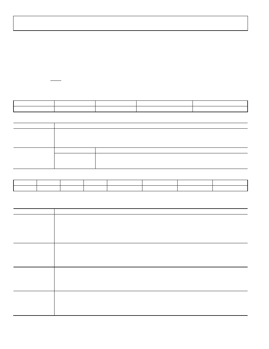
Table 25. Programming the Software Register
D15
D14
D13
D12
D11 to D0
1
0
User program
Reset code/SPI code
Table 26. Software Register Bit Descriptions
Bit Name
Description
User Program
This bit is mapped to Bit D11 of the status register. When this bit is set to 1, Bit D11 of the status register is set to 1.
When this bit is set to 0, Bit D11 of the status register is also set to 0. This feature can be used to ensure that the SPI
pins are working correctly by writing a known bit value to this register and then reading back Bit D11 from the
status register.
Reset Code/SPI Code
Option
Description
Reset code
Writing 0x555 to Bits[D11:D0] performs a software reset of the AD5735.
SPI code
If the watchdog timer feature is enabled, 0x195 must be written to the software register
(Bits[D11:D0]) within the programmed timeout period (see Table 22).
Table 27. Programming the DC-to-DC Control Register
D15
D14
D13
D12 to D7
D6
D5 to D4
D3 to D2
D1 to D0
0
1
X1
DC-DC comp
DC-DC phase
DC-DC freq
DC-DC MaxV
1 X = don’t care.
Table 28. DC-to-DC Control Register Bit Descriptions
Bit Name
Description
DC-DC Comp
Selects the internal compensation resistor or an external compensation resistor for the dc-to-dc converter. See the
0 = selects the internal 150 k compensation resistor (default).
1 = bypasses the internal compensation resistor. When this bit is set to 1, an external compensation resistor must
be used; this resistor is placed at the COMP
DCDC_x pin in series with the 10 nF dc-to-dc compensation capacitor to
ground. Typically, a resistor of ~50 k is recommended.
DC-DC Phase
User-programmable dc-to-dc converter phase (between channels).
00 = all dc-to-dc converters clock on the same edge (default).
01 = Channel A and Channel B clock on the same edge; Channel C and Channel D clock on the opposite edge.
10 = Channel A and Channel C clock on the same edge; Channel B and Channel D clock on the opposite edge.
11 = Channel A, Channel B, Channel C, and Channel D clock 90° out of phase from each other.
DC-DC Freq
Switching frequency for the dc-to-dc converter; this frequency is divided down from the internal 13 MHz oscillator
00 = 250 kHz ± 10%.
01 = 410 kHz ± 10% (default).
10 = 650 kHz ± 10%.
DC-DC MaxV
Maximum allowed V
BOOST_x voltage supplied by the dc-to-dc converter.
00 = 23 V + 1 V/1.5 V (default).
01 = 24.5 V ± 1 V.
10 = 27 V ± 1 V.
11 = 29.5 V ± 1 V.
相关PDF资料 |
PDF描述 |
|---|---|
| AD5044BRUZ | IC DAC QUAD 14BIT SPI 16TSSOP |
| MS3454W24-22S | CONN RCPT 4POS JAM NUT W/SCKT |
| ADV7125JSTZ330 | IC DAC VIDEO 3CH 330MHZ 48LQFP |
| VE-21N-MY-F2 | CONVERTER MOD DC/DC 18.5V 50W |
| LTC2625IGN#PBF | IC DAC 12BIT R-R OCT 16SSOP |
相关代理商/技术参数 |
参数描述 |
|---|---|
| AD5735ACPZ-REEL7 | 功能描述:IC DAC QUAD VOLT CUR 64LFCSP RoHS:是 类别:集成电路 (IC) >> 数据采集 - 数模转换器 系列:- 产品培训模块:Data Converter Fundamentals DAC Architectures 标准包装:750 系列:- 设置时间:7µs 位数:16 数据接口:并联 转换器数目:1 电压电源:双 ± 功率耗散(最大):100mW 工作温度:0°C ~ 70°C 安装类型:表面贴装 封装/外壳:28-LCC(J 形引线) 供应商设备封装:28-PLCC(11.51x11.51) 包装:带卷 (TR) 输出数目和类型:1 电压,单极;1 电压,双极 采样率(每秒):143k |
| AD5737 | 制造商:AD 制造商全称:Analog Devices 功能描述:Quad Channel, 16-Bit, Serial Input, 4-20mA Output DAC, Dynamic Power Control, HART Connectivity |
| AD5737_12 | 制造商:AD 制造商全称:Analog Devices 功能描述:Quad-Channel, 12-Bit, Serial Input, 4 mA to 20 mA Output |
| AD5737ACPZ | 功能描述:IC DAC QUAD 12BIT CUR 64-LFCSP RoHS:是 类别:集成电路 (IC) >> 数据采集 - 数模转换器 系列:- 标准包装:1 系列:- 设置时间:4.5µs 位数:12 数据接口:串行,SPI? 转换器数目:1 电压电源:单电源 功率耗散(最大):- 工作温度:-40°C ~ 125°C 安装类型:表面贴装 封装/外壳:8-SOIC(0.154",3.90mm 宽) 供应商设备封装:8-SOICN 包装:剪切带 (CT) 输出数目和类型:1 电压,单极;1 电压,双极 采样率(每秒):* 其它名称:MCP4921T-E/SNCTMCP4921T-E/SNRCTMCP4921T-E/SNRCT-ND |
| AD5737ACPZ-RL7 | 制造商:AD 制造商全称:Analog Devices 功能描述:Quad-Channel, 12-Bit, Serial Input, 4 mA to 20 mA Output |
发布紧急采购,3分钟左右您将得到回复。