参数资料
| 型号: | AD5735ACPZ |
| 厂商: | Analog Devices Inc |
| 文件页数: | 37/48页 |
| 文件大小: | 0K |
| 描述: | IC DAC QUAD VOLT CUR 64-LFCSP |
| 标准包装: | 1 |
| 设置时间: | 18µs |
| 位数: | 12 |
| 数据接口: | DSP,MICROWIRE?,QSPI?,串行,SPI? |
| 转换器数目: | 4 |
| 电压电源: | 模拟和数字,双 ± |
| 工作温度: | -40°C ~ 105°C |
| 安装类型: | 表面贴装 |
| 封装/外壳: | 64-VFQFN 裸露焊盘,CSP |
| 供应商设备封装: | 64-LFCSP-VQ(9x9) |
| 包装: | 托盘 |
| 输出数目和类型: | 4 电流,4 电压 |
| 采样率(每秒): | * |
第1页第2页第3页第4页第5页第6页第7页第8页第9页第10页第11页第12页第13页第14页第15页第16页第17页第18页第19页第20页第21页第22页第23页第24页第25页第26页第27页第28页第29页第30页第31页第32页第33页第34页第35页第36页当前第37页第38页第39页第40页第41页第42页第43页第44页第45页第46页第47页第48页
AD5735
Data Sheet
Rev. C | Page 42 of 48
DC-TO-DC CONVERTERS
The AD5735 contains four independent dc-to-dc converters.
These are used to provide dynamic control of the VBOOST_x supply
voltage for each channel (see Figure 71). Figure 77 shows the
discrete components needed for the dc-to-dc circuitry, and the
following sections describe component selection and operation
of this circuitry.
AVCC
LDCDC
DDCDC
CDCDC
4.7F
CFILTER
0.1F
RFILTER
CIN
SWx
VBOOST_x
≥10F
10
10H
09961-
077
Figure 77. DC-to-DC Circuit
Table 36. Recommended Components for a DC-to-DC Converter
Symbol
Component
Value
Manufacturer
L
DCDC
XAL4040-103
10 H
Coilcraft
C
DCDC
GRM32ER71H475KA88L
4.7 F
Murata
D
DCDC
PMEG3010BEA
0.285 V
F
NXP
It is recommended that a 10 , 100 nF low-pass RC filter be
placed after CDCDC. This filter consumes a small amount of power
but reduces the amount of ripple on the VBOOST_x supply.
DC-to-DC Converter Operation
The on-board dc-to-dc converters use a constant frequency, peak
current mode control scheme to step up an AVCC input of 4.5 V
to 5.5 V to drive the AD5735 output channel. These converters
are designed to operate in discontinuous conduction mode with
a duty cycle of <90% typical. Discontinuous conduction mode
refers to a mode of operation where the inductor current goes
to zero for an appreciable percentage of the switching cycle. The
dc-to-dc converters are nonsynchronous; that is, they require an
external Schottky diode.
DC-to-DC Converter Output Voltage
When a channel current output is enabled, the converter regulates
the VBOOST_x supply to 7.4 V (±5%) or (IOUT × RLOAD + Headroom),
whichever is greater (see Figure 51 for a plot of headroom
supplied vs. output current). In voltage output mode with the
output disabled, the converter regulates the VBOOST_x supply to
15 V (±5%). In current output mode with the output disabled,
the converter regulates the VBOOST_x supply to 7.4 V (±5%).
Within a channel, the VOUT_x and IOUT_x stages share a common
VBOOST_x supply; therefore, the outputs of the IOUT_x and VOUT_x
stages can be tied together (see the Voltage and Current Output
Pins on the Same Terminal section).
DC-to-DC Converter Settling Time
In current output mode, the settling time for a step greater than
~1 V (IOUT × RLOAD) is dominated by the settling time of the dc-to-
dc converter. The exception to this is when the required voltage at
the IOUT_x pin plus the compliance voltage is below 7.4 V (±5%).
Figure 47 shows a typical plot of the output settling time. This
plot is for a 1 k load. The settling time for smaller loads is faster.
The settling time for current steps less than 24 mA is also faster.
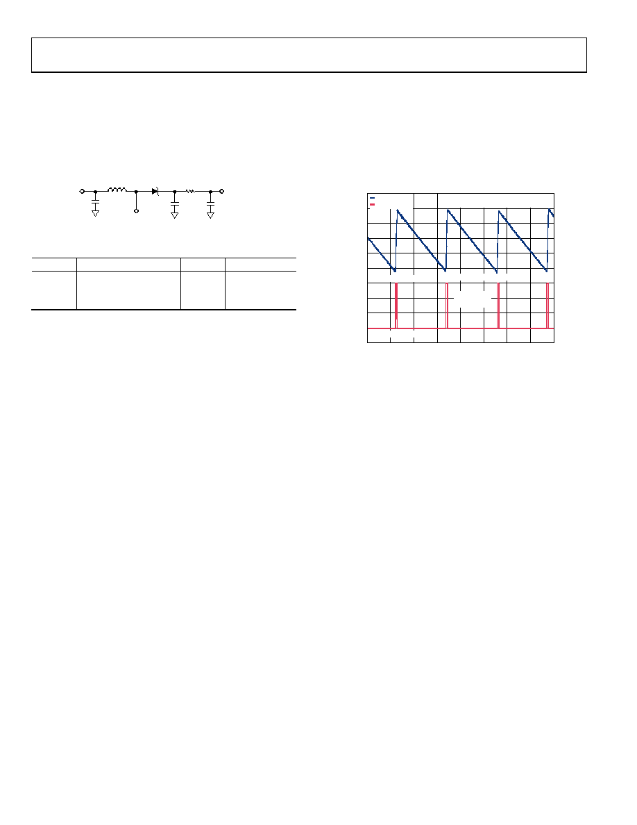
DC-to-DC Converter VMAX Functionality
The maximum VBOOST_x voltage is set in the dc-to-dc control
register (23 V, 24.5 V, 27 V, or 29.5 V; see Table 28). When the
maximum voltage is reached, the dc-to-dc converter is disabled,
and the VBOOST_x voltage is allowed to decay by ~0.4 V. After the
VBOOST_x voltage decays by ~0.4 V, the dc-to-dc converter is
reenabled, and the voltage ramps up again to VMAX, if still
required. This operation is shown in Figure 78.
28.6
28.7
28.8
28.9
29.0
29.1
29.2
29.3
29.4
29.5
29.6
0
0.5
1.0
1.5
2.0
2.5
3.0
3.5
4.0
V
B
OOS
T
_
x
VO
LT
A
G
E
(V)
TIME (ms)
VMAX
0mA TO 24mA RANGE, 24mA OUTPUT
OUTPUT UNLOADED
DC-DC MaxV BITS = 29.5V
DC-DCx BIT
DC-DCx BIT = 0
DC-DCx BIT = 1
f
SW = 410kHz
TA = 25°C
09961-
183
Figure 78. Operation on Reaching VMAX
As shown in Figure 78, the DC-DCx bit in the status register
is deasserted when the voltage decays to VMAX ~0.4 V.
DC-to-DC Converter On-Board Switch
The AD5735 contains a 0.425 internal switch. The switch
current is monitored on a pulse-by-pulse basis and is limited
to 0.8 A peak current.
DC-to-DC Converter Switching Frequency and Phase
The AD5735 dc-to-dc converter switching frequency can be
selected from the dc-to-dc control register (see Table 28). The
phasing of the channels can also be adjusted so that the dc-to-dc
converters can clock on different edges. For typical applications,
a 410 kHz frequency is recommended. At light loads (low output
current and small load resistor), the dc-to-dc converter enters a
pulse-skipping mode to minimize switching power dissipation.
DC-to-DC Converter Inductor Selection
For typical 4 mA to 20 mA applications, a 10 H inductor (such
as the XAL4040-103 from Coilcraft), combined with a switching
frequency of 410 kHz, allows up to 24 mA to be driven into a
load resistance of up to 1 k with an AVCC supply of 4.5 V to
5.5 V. It is important to ensure that the inductor can handle the
peak current without saturating, especially at the maximum
ambient temperature. If the inductor enters saturation mode,
efficiency decreases. The inductance value also drops during
saturation and may result in the dc-to-dc converter circuit not
being able to supply the required output power.
相关PDF资料 |
PDF描述 |
|---|---|
| AD5044BRUZ | IC DAC QUAD 14BIT SPI 16TSSOP |
| MS3454W24-22S | CONN RCPT 4POS JAM NUT W/SCKT |
| ADV7125JSTZ330 | IC DAC VIDEO 3CH 330MHZ 48LQFP |
| VE-21N-MY-F2 | CONVERTER MOD DC/DC 18.5V 50W |
| LTC2625IGN#PBF | IC DAC 12BIT R-R OCT 16SSOP |
相关代理商/技术参数 |
参数描述 |
|---|---|
| AD5735ACPZ-REEL7 | 功能描述:IC DAC QUAD VOLT CUR 64LFCSP RoHS:是 类别:集成电路 (IC) >> 数据采集 - 数模转换器 系列:- 产品培训模块:Data Converter Fundamentals DAC Architectures 标准包装:750 系列:- 设置时间:7µs 位数:16 数据接口:并联 转换器数目:1 电压电源:双 ± 功率耗散(最大):100mW 工作温度:0°C ~ 70°C 安装类型:表面贴装 封装/外壳:28-LCC(J 形引线) 供应商设备封装:28-PLCC(11.51x11.51) 包装:带卷 (TR) 输出数目和类型:1 电压,单极;1 电压,双极 采样率(每秒):143k |
| AD5737 | 制造商:AD 制造商全称:Analog Devices 功能描述:Quad Channel, 16-Bit, Serial Input, 4-20mA Output DAC, Dynamic Power Control, HART Connectivity |
| AD5737_12 | 制造商:AD 制造商全称:Analog Devices 功能描述:Quad-Channel, 12-Bit, Serial Input, 4 mA to 20 mA Output |
| AD5737ACPZ | 功能描述:IC DAC QUAD 12BIT CUR 64-LFCSP RoHS:是 类别:集成电路 (IC) >> 数据采集 - 数模转换器 系列:- 标准包装:1 系列:- 设置时间:4.5µs 位数:12 数据接口:串行,SPI? 转换器数目:1 电压电源:单电源 功率耗散(最大):- 工作温度:-40°C ~ 125°C 安装类型:表面贴装 封装/外壳:8-SOIC(0.154",3.90mm 宽) 供应商设备封装:8-SOICN 包装:剪切带 (CT) 输出数目和类型:1 电压,单极;1 电压,双极 采样率(每秒):* 其它名称:MCP4921T-E/SNCTMCP4921T-E/SNRCTMCP4921T-E/SNRCT-ND |
| AD5737ACPZ-RL7 | 制造商:AD 制造商全称:Analog Devices 功能描述:Quad-Channel, 12-Bit, Serial Input, 4 mA to 20 mA Output |
发布紧急采购,3分钟左右您将得到回复。