参数资料
| 型号: | AD5757ACPZ |
| 厂商: | Analog Devices Inc |
| 文件页数: | 19/44页 |
| 文件大小: | 0K |
| 描述: | IC DAC 16BIT QUAD 64-LFCSP |
| 特色产品: | AD5755 / AD5755-1 / AD5757 DACs |
| 标准包装: | 1 |
| 设置时间: | 15µs |
| 位数: | 16 |
| 数据接口: | DSP,MICROWIRE?,QSPI?,串行,SPI? |
| 转换器数目: | 4 |
| 电压电源: | 模拟和数字 |
| 工作温度: | -40°C ~ 105°C |
| 安装类型: | 表面贴装 |
| 封装/外壳: | 64-VFQFN 裸露焊盘,CSP |
| 供应商设备封装: | 64-LFCSP-VQ(9x9) |
| 包装: | 管件 |
| 输出数目和类型: | * |
| 采样率(每秒): | * |
第1页第2页第3页第4页第5页第6页第7页第8页第9页第10页第11页第12页第13页第14页第15页第16页第17页第18页当前第19页第20页第21页第22页第23页第24页第25页第26页第27页第28页第29页第30页第31页第32页第33页第34页第35页第36页第37页第38页第39页第40页第41页第42页第43页第44页
AD5757
Data Sheet
Rev. D | Page 26 of 44
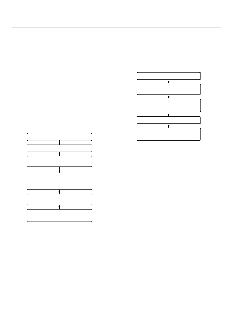
PROGRAMMING SEQUENCE TO WRITE/ENABLE
THE OUTPUT CORRECTLY
To correctly write to and set up the part from a power-on
condition, use the following sequence:
1. Perform a hardware or software reset after initial power-on.
2. The dc-to-dc converter supply block must be configured.
Set the dc-to-dc switching frequency, maximum output
voltage allowed, and the phase that the four dc-to-dc
channels clock at.
3. Configure the DAC control register on a per channel basis.
The output range is selected, and the dc-to-dc converter
block is enabled (DC_DC bit). Other control bits can be
configured at this point. Set the INT_ENABLE bit;
however, the output enable bit (OUTEN) should not be set.
4. Write the required code to the DAC data register. This
implements a full DAC calibration internally. Allow at least
200 s before Step 5 for reduced output glitch.
5. Write to the DAC control register again to enable the
output (set the OUTEN bit).
A flowchart of this sequence is shown in Figure 51.
POWER ON.
STEP 1: PERFORM A SOFTWARE/HARDWARE RESET.
STEP 4: WRITE TO EACH/ALL DAC DATA REGISTERS.
ALLOW AT LEAST 200s BETWEEN STEP 3
AND STEP 5 FOR REDUCED OUTPUT GLITCH.
STEP 2: WRITE TO DC-TO-DC CONTROL REGISTER TO
SET DC-TO-DC CLOCK FREQUENCY, PHASE,
AND MAXIMUM VOLTAGE.
STEP 3: WRITE TO DAC CONTROL REGISTER. SELECT
THE DAC CHANNEL AND OUTPUT RANGE.
SET THE DC_DC BIT AND OTHER CONTROL
BITS AS REQUIRED. SET THE INT_ENABLE BIT
BUT DO NOT SELECT THE OUTEN BIT.
STEP 5: WRITE TO DAC CONTROL REGISTER. RELOAD
SEQUENCE AS IN STEP 3 ABOVE. THIS TIME
SELECT THE OUTEN BIT TO ENABLE
THE OUTPUT.
09225-
073
Figure 51. Programming Sequence for Enabling the Output Correctly
CHANGING AND REPROGRAMMING THE RANGE
When changing between ranges, the same sequence as
described in the Programming Sequence to Write/Enable the
Output Correctly section should be used. It is recommended to
set the range to zero scale prior to disabling the output. Because
the dc-to-dc switching frequency, maximum voltage, and phase
have already been selected, there is no need to reprogram these.
A flowchart of this sequence is shown in Figure 52.
CHANNEL’S OUTPUT IS ENABLED.
STEP 3: WRITE VALUE TO THE DAC DATA REGISTER.
STEP 1: WRITE TO CHANNEL’S DAC DATA
REGISTER. SET THE OUTPUT
TO 0V (ZERO OR MIDSCALE).
STEP 2: WRITE TO DAC CONTROL REGISTER.
DISABLE THE OUTPUT (OUTEN = 0), AND
SET THE NEW OUTPUT RANGE. KEEP THE
DC_DC BIT AND THE INT_ENABLE BIT SET.
STEP 4: WRITE TO DAC CONTROL REGISTER.
RELOAD SEQUENCE AS IN STEP 2 ABOVE.
THIS TIME SELECT THE OUTEN BIT TO
ENABLE THE OUTPUT.
09225-
074
Figure 52. Steps for Changing the Output Range
相关PDF资料 |
PDF描述 |
|---|---|
| MS3122E16-23S | CONN RCPT 23POS BOX MNT W/SCKT |
| MS27497T18A32PLC | CONN HSG RCPT 32POS WALL MT PINS |
| AD7225KNZ | IC DAC 8BIT QUAD W/AMP 24DIP |
| VE-2WL-MY-F4 | CONVERTER MOD DC/DC 28V 50W |
| AD7537KRZ | IC DAC 12BIT DUAL MULT 24SOIC |
相关代理商/技术参数 |
参数描述 |
|---|---|
| AD5757ACPZ-REEL7 | 功能描述:IC DAC 16BIT QUAD IOUT 64LFCSP RoHS:是 类别:集成电路 (IC) >> 数据采集 - 数模转换器 系列:- 产品培训模块:Data Converter Fundamentals DAC Architectures 标准包装:750 系列:- 设置时间:7µs 位数:16 数据接口:并联 转换器数目:1 电压电源:双 ± 功率耗散(最大):100mW 工作温度:0°C ~ 70°C 安装类型:表面贴装 封装/外壳:28-LCC(J 形引线) 供应商设备封装:28-PLCC(11.51x11.51) 包装:带卷 (TR) 输出数目和类型:1 电压,单极;1 电压,双极 采样率(每秒):143k |
| AD5757X | 制造商:AD 制造商全称:Analog Devices 功能描述:Quad Channel, 16-Bit, Serial Input, 4-20mA Output DAC, Dynamic Power Control, HART Connectivity |
| AD575JD | 制造商:未知厂家 制造商全称:未知厂家 功能描述:Analog-to-Digital Converter, 10-Bit |
| AD575JN | 制造商:未知厂家 制造商全称:未知厂家 功能描述:Analog-to-Digital Converter, 10-Bit |
| AD575KD | 制造商:未知厂家 制造商全称:未知厂家 功能描述:Analog-to-Digital Converter, 10-Bit |
发布紧急采购,3分钟左右您将得到回复。