参数资料
| 型号: | AD5757ACPZ |
| 厂商: | Analog Devices Inc |
| 文件页数: | 36/44页 |
| 文件大小: | 0K |
| 描述: | IC DAC 16BIT QUAD 64-LFCSP |
| 特色产品: | AD5755 / AD5755-1 / AD5757 DACs |
| 标准包装: | 1 |
| 设置时间: | 15µs |
| 位数: | 16 |
| 数据接口: | DSP,MICROWIRE?,QSPI?,串行,SPI? |
| 转换器数目: | 4 |
| 电压电源: | 模拟和数字 |
| 工作温度: | -40°C ~ 105°C |
| 安装类型: | 表面贴装 |
| 封装/外壳: | 64-VFQFN 裸露焊盘,CSP |
| 供应商设备封装: | 64-LFCSP-VQ(9x9) |
| 包装: | 管件 |
| 输出数目和类型: | * |
| 采样率(每秒): | * |
第1页第2页第3页第4页第5页第6页第7页第8页第9页第10页第11页第12页第13页第14页第15页第16页第17页第18页第19页第20页第21页第22页第23页第24页第25页第26页第27页第28页第29页第30页第31页第32页第33页第34页第35页当前第36页第37页第38页第39页第40页第41页第42页第43页第44页
Data Sheet
AD5757
Rev. D | Page 41 of 44
TRANSIENT VOLTAGE PROTECTION
The AD5757 contains ESD protection diodes that prevent dam-
age from normal handling. The industrial control environment
can, however, subject I/O circuits to much higher transients. To
protect the AD5757 from excessively high voltage transients,
external power diodes and a surge current limiting resistor (RP)
The two protection diodes and the resistor (RP) must have appro-
priate power ratings.
RLOAD
R
D1
D2
P
AD5757
VBOOST_x
IOUT_x
AGND
CDCDC
4.7F
CFILTER
0.1F
RFILTER
10
(FROM
DC-TO-DC
CONVERTER)
09225-
013
Figure 63. Output Transient Voltage Protection
Additional protection can be provided using transient voltage
suppressors (TVSs), also referred to as transorbs. These compo-
nents are available as unidirectional suppressors, which protect
against positive high voltage transients, and as bidirectional
suppressors, which protect against both positive and negative
high voltage transients. Transient voltage suppressors are avail-
able in a wide range of standoff and breakdown voltage ratings.
The TVS should be sized with the lowest breakdown voltage
possible while not conducting in the functional range of the
current output.
It is recommended that all field connected nodes be protected.
MICROPROCESSOR INTERFACING
Microprocessor interfacing to the AD5757 is via a serial bus that
uses a protocol compatible with microcontrollers and DSP
processors. The communications channel is a 3-wire minimum
interface consisting of a clock signal, a data signal, and a latch
signal. The AD5757 requires a 24-bit data-word with data valid
on the falling edge of SCLK.
The DAC output update is initiated on either the rising edge of
LDAC or, if LDAC is held low, on the rising edge of SYNC. The
contents of the registers can be read using the readback function.
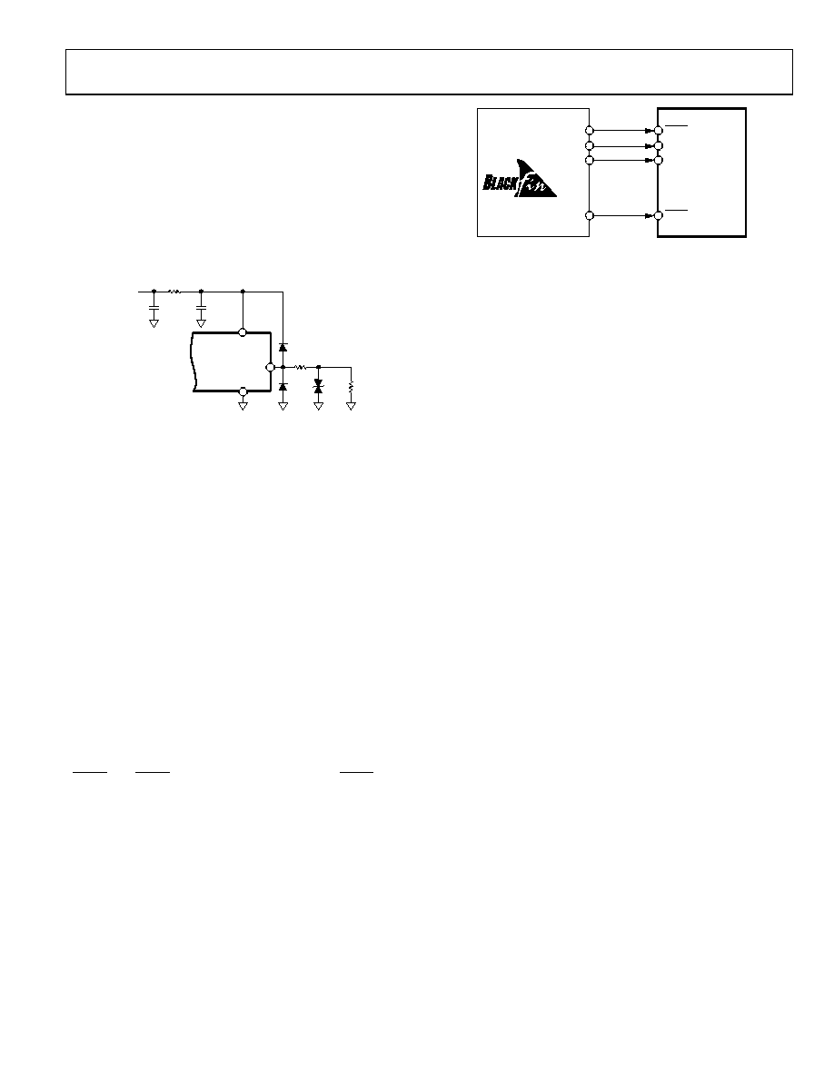
AD5757-TO-ADSP-BF527 INTERFACE
The AD5757 can be connected directly to the SPORT interface
of the ADSP-BF527, an Analog Devices, Inc., Blackfin DSP.
Figure 64 shows how the SPORT interface can be connected to
control the AD5757.
AD5757
SYNC
SCLK
SDIN
LDAC
SPORT_TFS
SPORT_TSCK
SPORT_DTO
GPIO0
ADSP-BF527
09225-
080
Figure 64. AD5757-to-ADSP-BF527 SPORT Interface
LAYOUT GUIDELINES
Grounding
In any circuit where accuracy is important, careful consideration
of the power supply and ground return layout helps to ensure
the rated performance. The printed circuit board on which the
AD5757 is mounted should be designed so that the analog and
digital sections are separated and confined to certain areas of the
board. If the AD5757 is in a system where multiple devices
require an AGND-to-DGND connection, the connection should
be made at one point only. The star ground point should be
established as close as possible to the device.
The GNDSWx and ground connection for the AVCC supply are
referred to as PGND. PGND should be confined to certain areas
of the board, and the PGND-to-AGND connection should be
made at one point only.
Supply Decoupling
The AD5757 should have ample supply bypassing of 10 F
in parallel with 0.1 F on each supply located as close to the
package as possible, ideally right up against the device. The
10 F capacitors are the tantalum bead type. The 0.1 F capaci-
tor should have low effective series resistance (ESR) and low
effective series inductance (ESL), such as the common ceramic
types, which provide a low impedance path to ground at high
frequencies to handle transient currents due to internal logic
switching.
Traces
The power supply lines of the AD5757 should use as large a
trace as possible to provide low impedance paths and reduce the
effects of glitches on the power supply line. Fast switching signals
such as clocks should be shielded with digital ground to prevent
radiating noise to other parts of the board and should never be
run near the reference inputs. A ground line routed between the
SDIN and SCLK lines helps reduce crosstalk between them (not
required on a multilayer board that has a separate ground plane,
but separating the lines helps). It is essential to minimize noise
on the REFIN line because it couples through to the DAC output.
Avoid crossover of digital and analog signals. Traces on
opposite sides of the board should run at right angles to each
other. This reduces the effects of feedthrough on the board. A
microstrip technique is by far the best but not always possible
with a double-sided board. In this technique, the component
side of the board is dedicated to ground plane, whereas signal
traces are placed on the solder side.
相关PDF资料 |
PDF描述 |
|---|---|
| MS3122E16-23S | CONN RCPT 23POS BOX MNT W/SCKT |
| MS27497T18A32PLC | CONN HSG RCPT 32POS WALL MT PINS |
| AD7225KNZ | IC DAC 8BIT QUAD W/AMP 24DIP |
| VE-2WL-MY-F4 | CONVERTER MOD DC/DC 28V 50W |
| AD7537KRZ | IC DAC 12BIT DUAL MULT 24SOIC |
相关代理商/技术参数 |
参数描述 |
|---|---|
| AD5757ACPZ-REEL7 | 功能描述:IC DAC 16BIT QUAD IOUT 64LFCSP RoHS:是 类别:集成电路 (IC) >> 数据采集 - 数模转换器 系列:- 产品培训模块:Data Converter Fundamentals DAC Architectures 标准包装:750 系列:- 设置时间:7µs 位数:16 数据接口:并联 转换器数目:1 电压电源:双 ± 功率耗散(最大):100mW 工作温度:0°C ~ 70°C 安装类型:表面贴装 封装/外壳:28-LCC(J 形引线) 供应商设备封装:28-PLCC(11.51x11.51) 包装:带卷 (TR) 输出数目和类型:1 电压,单极;1 电压,双极 采样率(每秒):143k |
| AD5757X | 制造商:AD 制造商全称:Analog Devices 功能描述:Quad Channel, 16-Bit, Serial Input, 4-20mA Output DAC, Dynamic Power Control, HART Connectivity |
| AD575JD | 制造商:未知厂家 制造商全称:未知厂家 功能描述:Analog-to-Digital Converter, 10-Bit |
| AD575JN | 制造商:未知厂家 制造商全称:未知厂家 功能描述:Analog-to-Digital Converter, 10-Bit |
| AD575KD | 制造商:未知厂家 制造商全称:未知厂家 功能描述:Analog-to-Digital Converter, 10-Bit |
发布紧急采购,3分钟左右您将得到回复。