- 您现在的位置:买卖IC网 > PDF目录373890 > AD6623ABC (ANALOG DEVICES INC) 4-Channel, 104 MSPS Digital Transmit Signal Processor TSP PDF资料下载
参数资料
| 型号: | AD6623ABC |
| 厂商: | ANALOG DEVICES INC |
| 元件分类: | 通信及网络 |
| 英文描述: | 4-Channel, 104 MSPS Digital Transmit Signal Processor TSP |
| 中文描述: | SPECIALTY TELECOM CIRCUIT, PBGA196 |
| 封装: | CSPBGA-196 |
| 文件页数: | 25/40页 |
| 文件大小: | 381K |
| 代理商: | AD6623ABC |
第1页第2页第3页第4页第5页第6页第7页第8页第9页第10页第11页第12页第13页第14页第15页第16页第17页第18页第19页第20页第21页第22页第23页第24页当前第25页第26页第27页第28页第29页第30页第31页第32页第33页第34页第35页第36页第37页第38页第39页第40页
REV. 0
AD6623
–25–
frequencies solely by spectral inversion. The digital IF is calcu-
lated using the equation:
NCO
frequency
IF
NCO
=
×
2
32
where:
NCO_frequency
is the value written to 0xn02,
f
IF
is the desired intermediate frequency, and
f
NCO
is f
CLK
/2 for complex outputs and f
CLK
for real outputs.
Phase Dither
The AD6623 provides a phase dither option for improving the
spurious performance of the NCO. Phase dither is enabled by
writing a
“
1
”
to Bit 3 of Channel Register 0xn01. When phase
dither is enabled, spurs due to phase truncation in the NCO are
randomized. The choice of whether phase dither is used in a system
will ultimately be decided by the system goals and the choice of IF
frequency. The 18 most significant bits of the phase accumulator
are used by the angle to Cartesian conversion. If the NCO frequency
has all zeroes below the 18
th
bit, then phase dither has no effect.
If the fraction below the 18
th
bit is near a 1/2 or 1/3 of the 18
th
bit, then spurs will accumulate separated from the IF by 1/2 or
1/3 of the CLK frequency. The smaller the denominator of this
residual fraction, the larger the spurs due to phase truncation will
be. If the phase truncation spurs are unacceptably high for a given
frequency, then the phase dither can reduce these at the penalty
of a slight elevation in total error energy. If the phase truncation
spurs are small, then phase dither will not be effective in reducing
them further, but a slight elevation in total error energy will occur.
Amplitude Dither
Amplitude dither can also be used to improve spurious performance
of the NCO. Amplitude dither is enabled by writing a
“
1
”
to Bit 4
of Channel Register at 0xn01. When enabled, amplitude dither
can reduce spurs due to truncation at the input to the QAM. If
the entire frequency word is close to a fraction that has a small
denominator, the spurs due to amplitude truncation will be large
and amplitude dither will spread these spurs effectively. Amplitude
dither also will increase the total error energy by approximately
3 dB. For this reason amplitude dither should be used judiciously.
Phase Offset
The phase offset (Channel Register 0xn04) adds an offset to the
phase accumulator of the NCO. This is a 16-bit register that is
interpreted as a 16-bit unsigned integer. Phase offset ranges
from 0 to nearly 2 radians with a resolution of /32768 radians.
f
f
_
(21)
This register allows multiple NCOs to be synchronized to produce
sine waves with a known phase relationship.
NCO Frequency Update and Phase Offset Update Hold-Off
Counters
The update of both the NCO frequency and phase offset
can be
synchronized with internal Hold-Off counters. Both of
these
counters are 16-bit unsigned integers and are clocked at
the master
CLK
rate. These Hold-Off counters used in conjunc-
tion with the
frequency or phase offset registers, allow beam
forming and frequency
hopping. See the Synchronization section
of the data sheet for additional
details. The NCO phase can also
be cleared on Sync (set to 0x0000)
by setting Bit 2 of Channel
Register 0xn01 high.
NCO Control Scale
The output of the NCO can be scaled in four steps of 6 dB each
via Channel Register 0xn01, Bits 1
–
0. Table XV show a break-
down of the NCO Control Scale. The NCO always has loss to
accommodate the possibility that both the I and Q inputs may
reach full-scale simultaneously, resulting in a 3 dB input magnitude.
Table XV. NCO Control Scale
0xn01 Bit 1
0xn01 Bit 0
NCO Output Level
0
0
1
1
0
1
0
1
–
6 dB (no attenuation)
–
12 dB attenuation
–
18 dB attenuation
–
24 dB attenuation
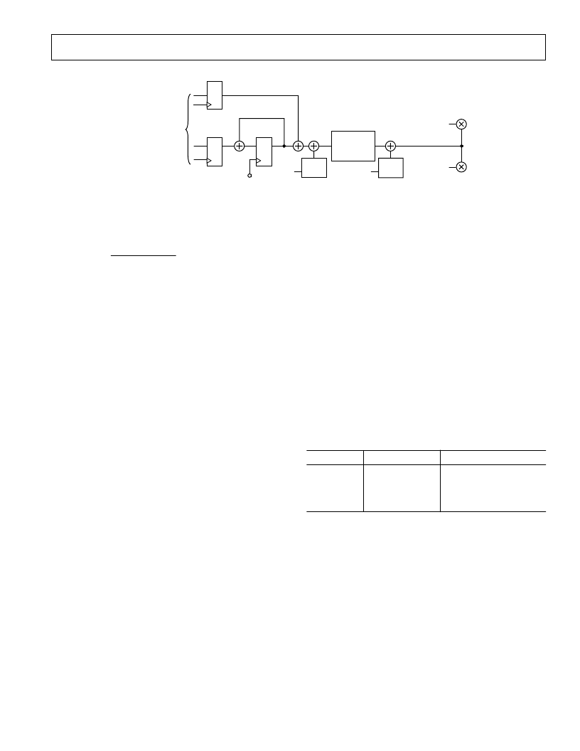
SUMMATION BLOCK
The Summation Block of the AD6623 serves to combine the
outputs of each channel to create a composite multicarrier signal.
The four channels are summed together and the result is then
added with the 18-bit Wideband Input Bus (IN[17:0]). The final
summation is then driven on the 18-bit Wideband Output Bus
(OUT[17:0]) on the rising edge of the high speed clock. If the
OEN input is high then this output bus is three-stated. If the OEN
input is low then this bus will be driven by the summed data.
The OEN is active high to allow the Wideband Output Bus to
be connected to other busses without using extra logic. Most
other
busses (like 374 type registers) require a low output enable,
which is
opposite of the AD6623 OEN, thus eliminating extra circuitry.
The wideband parallel input IN[17:0] is defined as bidirectional,
to support dual parallel outputs. Each parallel output produces
the sum of two of the four internal TSPs and AD6623
that can
32
32
Q
D
PN
GEN.
NCO
FREQUENCY
WORD
16
PHASE
OFFSET
16
32
32
Q
D
ANGLE TO
CARTESIAN
CONVERSION
PN
GEN.
I DATA FROM
CIC5
Q DATA FROM
CIC5
I
Q
I, Q
CLK
ON
OFF
ON
OFF
32
32
MICROPROCESSOR
INTERFACE
Figure 31. Numerically Controlled Oscillator and QAM Mixer
相关PDF资料 |
PDF描述 |
|---|---|
| AD6623AS | 4-Channel, 104 MSPS Digital Transmit Signal Processor TSP |
| AD6623PCB | 4-Channel, 104 MSPS Digital Transmit Signal Processor TSP |
| AD6624AS | Four-Channel, 80 MSPS Digital Receive Signal Processor (RSP) |
| AD6624A | Four-Channel, 100 MSPS Digital Receive Signal Processor (RSP) |
| AD6624AABC | Four-Channel, 100 MSPS Digital Receive Signal Processor (RSP) |
相关代理商/技术参数 |
参数描述 |
|---|---|
| AD6623ABCZ | 制造商:Analog Devices 功能描述:Signal Processor 196-Pin CSP-BGA |
| AD6623AS | 制造商:Analog Devices 功能描述:Signal Processor 128-Pin MQFP 制造商:Rochester Electronics LLC 功能描述:4 CHANNEL, 104 MSPS DIGITAL TSP - Bulk |
| AD6623ASZ | 功能描述:IC TSP 4CHAN 104MSPS 128MQFP RoHS:是 类别:集成电路 (IC) >> 接口 - 专用 系列:- 特色产品:NXP - I2C Interface 标准包装:1 系列:- 应用:2 通道 I²C 多路复用器 接口:I²C,SM 总线 电源电压:2.3 V ~ 5.5 V 封装/外壳:16-TSSOP(0.173",4.40mm 宽) 供应商设备封装:16-TSSOP 包装:剪切带 (CT) 安装类型:表面贴装 产品目录页面:825 (CN2011-ZH PDF) 其它名称:568-1854-1 |
| AD6623BC/PCB | 制造商:AD 制造商全称:Analog Devices 功能描述:4-Channel, 104 MSPS Digital Transmit Signal Processor TSP |
| AD6623PCB | 制造商:AD 制造商全称:Analog Devices 功能描述:4-Channel, 104 MSPS Digital Transmit Signal Processor TSP |
发布紧急采购,3分钟左右您将得到回复。