- 您现在的位置:买卖IC网 > PDF目录373890 > AD6624AABC (ANALOG DEVICES INC) Four-Channel, 100 MSPS Digital Receive Signal Processor (RSP) PDF资料下载
参数资料
| 型号: | AD6624AABC |
| 厂商: | ANALOG DEVICES INC |
| 元件分类: | 通信及网络 |
| 英文描述: | Four-Channel, 100 MSPS Digital Receive Signal Processor (RSP) |
| 中文描述: | SPECIALTY TELECOM CIRCUIT, PBGA196 |
| 封装: | PLASTIC, BGA-196 |
| 文件页数: | 20/40页 |
| 文件大小: | 636K |
| 代理商: | AD6624AABC |
第1页第2页第3页第4页第5页第6页第7页第8页第9页第10页第11页第12页第13页第14页第15页第16页第17页第18页第19页当前第20页第21页第22页第23页第24页第25页第26页第27页第28页第29页第30页第31页第32页第33页第34页第35页第36页第37页第38页第39页第40页
REV. 0
AD6624A
–20–
Bit 11 of this register is used to invert the external exponent
before internal calculation. This bit should be set HIGH for
gain-ranging ADCs that use an increasing exponent to represent
an increasing signal level. This bit should be set LOW for gain-
ranging ADCs that use a decreasing exponent for representing
an increasing signal level.
In applications that do not require the features of the rCIC2,
it may be bypassed by setting the L/M ratio to 1/1. This effectively
bypasses all circuitry of the rCIC2 except the scaling, which
is still effectual.
FIFTH ORDER CASCADED INTEGRATOR COMB FILTER
The third signal processing stage, CIC5, implements a sharper
fixed-coefficient, decimating filter than CIC2. The input rate to
this filter is f
SAMP2
. The maximum input rate is given by Equa-
tion 9. N
CH
equals two for Diversity Channel Real input mode;
otherwise N
CH
equals one. In order to satisfy this equation, M
CIC2
can be increased, N
CH
can be reduced, or f
CLK
can be increased
(reference fractional rate input timing described in the Input
Timing section).
f
f
N
SAMP
CLK
CH
2
≤
(9)
The decimation ratio, M
CIC5
, may be programmed from 2 to 32
(all integer values). The frequency response of the filter is given
by Equation 10. The gain and passband droop of CIC5 should
be calculated by these equations. Both parameters may be com-
pensated for in the RCF stage.
H( )
z
–
z
S
M
CIC
CIC
–
1
–
–
=
×
+
1
2
1
5
5
5
1
5
(10)
H( )
M
f
f
f
f
S
CIC
SAMP
SAMP
CIC
sin
sin
=
×
×
+
1
2
5
5
5
2
2
5
π
π
The scale factor,
S
CIC
5
is a programmable unsigned integer
between 0 and 20. It serves to control the attenuation of the
data into the CIC5 stage in 6 dB increments. For the best
dynamic range, S
CIC5
should be set to the smallest value possible
(lowest attenuation) without creating an overflow condition.
This can be safely accomplished using Equation 11, where
OL
rCIC2
is the largest fraction of full scale possible at the input
to this filter stage. This value is output from the rCIC2 stage,
then pipelined into the CIC5.
(
=
(
+
S
ceil
M
OL
OL
M
OL
CIC
CIC
rCIC
CIC
CIC
S
rCIC
CIC
5
5
5
2
5
5
5
5
2
5
2
5
=
×
)
)
×
log (
)
–
(11)
The output rate of this stage is given by Equation 12.
f
f
M
SAMP
SAMP
CIC
5
2
5
≤
(12)
CIC5 Rejection
Table IV illustrates the amount of bandwidth in percentage of
the clock rate that can be protected with various decimation
rates and alias rejection specifications. The maximum input rate
into the CIC5 is 80 MHz when the rC1C2 decimates by one.
As in Table III, these are the 1/2 bandwidth characteristics of
the CIC5. Note that the CIC5 stage can protect a much wider
band than the CIC2 for any given rejection.
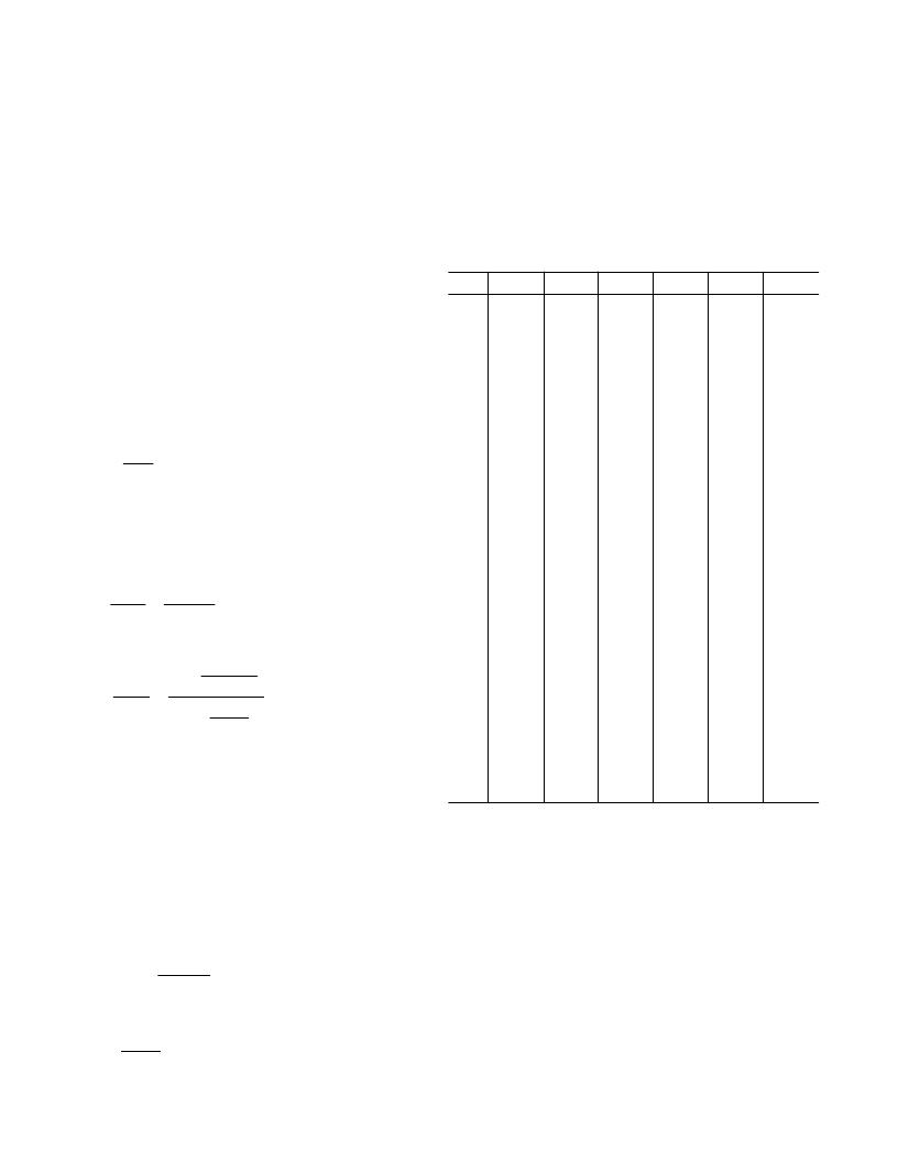
Table IV. SSB CIC5 Alias Rejection Table (f
SAMP2
= 1)
M
CIC5
2
3
4
5
6
7
8
9
10
11
12
13
14
15
16
17
18
19
20
21
22
23
24
25
26
27
28
29
30
31
32
–50 dB –60 dB
–70 dB
–80 dB –90 dB
–100 dB
10.227
7.924
6.213
5.068
4.267
3.68
3.233
2.881
2.598
2.365
2.17
2.005
1.863
1.74
1.632
1.536
1.451
1.375
1.307
1.245
1.188
1.137
1.09
1.046
1.006
0.969
0.934
0.902
0.872
0.844
0.818
8.078
6.367
5.022
4.107
3.463
2.989
2.627
2.342
2.113
1.924
1.765
1.631
1.516
1.416
1.328
1.25
1.181
1.119
1.064
1.013
0.967
0.925
0.887
0.852
0.819
0.789
0.761
0.734
0.71
0.687
0.666
6.393
5.11
4.057
3.326
2.808
2.425
2.133
1.902
1.716
1.563
1.435
1.326
1.232
1.151
1.079
1.016
0.96
0.91
0.865
0.824
0.786
0.752
0.721
0.692
0.666
0.641
0.618
0.597
0.577
0.559
0.541
5.066
4.107
3.271
2.687
2.27
1.962
1.726
1.54
1.39
1.266
1.162
1.074
0.998
0.932
0.874
0.823
0.778
0.737
0.701
0.667
0.637
0.61
0.584
0.561
0.54
0.52
0.501
0.484
0.468
0.453
0.439
4.008
3.297
2.636
2.17
1.836
1.588
1.397
1.247
1.125
1.025
0.941
0.87
0.809
0.755
0.708
0.667
0.63
0.597
0.568
0.541
0.516
0.494
0.474
0.455
0.437
0.421
0.406
0.392
0.379
0.367
0.355
3.183
2.642
2.121
1.748
1.48
1.281
1.128
1.007
0.909
0.828
0.76
0.703
0.653
0.61
0.572
0.539
0.509
0.483
0.459
0.437
0.417
0.399
0.383
0.367
0.353
0.34
0.328
0.317
0.306
0.297
0.287
This table helps to calculate an upper bound on decimation,
M
CIC5
, given the desired filter characteristics.
RAM COEFFICIENT FILTER
The final signal processing stage is a sum-of-products decimat-
ing filter with programmable coefficients (see Figure 27). The
data memories I-RAM and Q-RAM store the 160 most recent
complex samples from the previous filter stage with 20-bit
resolution. The coefficient memory, CMEM, stores up to 256
coefficients with 20-bit resolution. On every CLK cycle, one tap
for I and one tap for Q are calculated using the same coefficients.
The RCF output consists of 24-bit data bits.
相关PDF资料 |
PDF描述 |
|---|---|
| AD6630AR-REEL | Differential, Low Noise IF Gain Block with Output Clamping |
| AD6630AR | Differential, Low Noise IF Gain Block with Output Clamping |
| AD6630PCB | Differential, Low Noise IF Gain Block with Output Clamping |
| AD6630R | Differential, Low Noise IF Gain Block with Output Clamping |
| AD6633 | Multichannel Digital Upconverter with VersaCREST Crest Reduction Engine |
相关代理商/技术参数 |
参数描述 |
|---|---|
| AD6624AABCZ | 功能描述:DIGITAL SIGNAL PROC 196 CSP-BGA RoHS:是 类别:集成电路 (IC) >> 专用 IC 系列:* 产品培训模块:Lead (SnPb) Finish for COTS Obsolescence Mitigation Program 标准包装:1 系列:- 类型:调帧器 应用:数据传输 安装类型:表面贴装 封装/外壳:400-BBGA 供应商设备封装:400-PBGA(27x27) 包装:散装 |
| AD6624AS | 制造商:AD 制造商全称:Analog Devices 功能描述:Four-Channel, 80 MSPS Digital Receive Signal Processor (RSP) |
| AD6624AS/PCB | 制造商:AD 制造商全称:Analog Devices 功能描述:Four-Channel, 100 MSPS Digital Receive Signal Processor (RSP) |
| AD6624S/PCB | 制造商:AD 制造商全称:Analog Devices 功能描述:Four-Channel, 80 MSPS Digital Receive Signal Processor (RSP) |
| AD662AQ | 制造商:未知厂家 制造商全称:未知厂家 功能描述:12-Bit Digital-to-Analog Converter |
发布紧急采购,3分钟左右您将得到回复。