- 您现在的位置:买卖IC网 > PDF目录10297 > AD7192BRUZ-REEL (Analog Devices Inc)IC ADC 24BIT 2CH SD 24-TSSOP PDF资料下载
参数资料
| 型号: | AD7192BRUZ-REEL |
| 厂商: | Analog Devices Inc |
| 文件页数: | 13/41页 |
| 文件大小: | 0K |
| 描述: | IC ADC 24BIT 2CH SD 24-TSSOP |
| 设计资源: | Precision Weigh Scale Design Using AD7192 with Internal PGA (CN0119) |
| 标准包装: | 2,500 |
| 位数: | 24 |
| 采样率(每秒): | 4.8k |
| 数据接口: | DSP,MICROWIRE?,QSPI?,串行,SPI? |
| 转换器数目: | 1 |
| 电压电源: | 模拟和数字 |
| 工作温度: | -40°C ~ 105°C |
| 安装类型: | 表面贴装 |
| 封装/外壳: | 24-TSSOP(0.173",4.40mm 宽) |
| 供应商设备封装: | 24-TSSOP |
| 包装: | 带卷 (TR) |
| 输入数目和类型: | 2 个差分,单极;2 个差分,双极;4 个伪差分,单极;4 个伪差分,双极 |
第1页第2页第3页第4页第5页第6页第7页第8页第9页第10页第11页第12页当前第13页第14页第15页第16页第17页第18页第19页第20页第21页第22页第23页第24页第25页第26页第27页第28页第29页第30页第31页第32页第33页第34页第35页第36页第37页第38页第39页第40页第41页
AD7192
Rev. A | Page 19 of 40
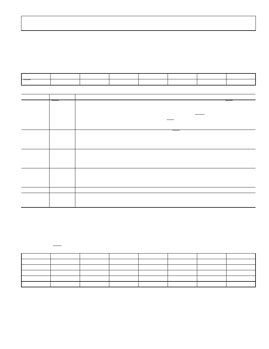
STATUS REGISTER
(RS2, RS1, RS0 = 0, 0, 0; Power-On/Reset = 0x80)
The status register is an 8-bit read-only register. To access the ADC status register, the user must write to the communications register,
select the next operation to be a read, and load Bit RS2, Bit RS1, and Bit RS0 with 0. Table 16 outlines the bit designations for the status
register. SR0 through SR7 indicate the bit locations, SR denoting that the bits are in the status register. SR7 denotes the first bit of the data
stream. The number in parentheses indicates the power-on/reset default status of that bit.
SR7
SR6
SR5
SR4
SR3
SR2
SR1
SR0
RDY(1)
ERR(0)
NOREF(0)
PARITY(0)
0(0)
CHD2(0)
CHD1(0)
CHD0(0)
Table 16. Status Register Bit Designations
Bit Location
Bit Name
Description
SR7
RDY
Ready bit for the ADC. This bit is cleared when data is written to the ADC data register. The RDY bit is set
automatically after the ADC data register is read, or a period of time before the data register is updated,
with a new conversion result to indicate to the user that the conversion data should not be read. It is also
set when the part is placed in power-down mode or idle mode or when SYNC is taken low.
The end of a conversion is also indicated by the DOUT/RDY pin. This pin can be used as an alternative to
the status register for monitoring the ADC for conversion data.
SR6
ERR
ADC error bit. This bit is written to at the same time as the RDY bit. This bit is set to indicate that the result
written to the ADC data register is clamped to all 0s or all 1s. Error sources include overrange or under-
range or the absence of a reference voltage. This bit is cleared when the result written to the data register is
within the allowed analog input range again.
SR5
NOREF
No external reference bit. This bit is set to indicate that the selected reference (REFIN1 or REFIN2) is at a
voltage that is below a specified threshold. When set, conversion results are clamped to all 1s. This bit is
cleared to indicate that a valid reference is applied to the selected reference pins. The NOREF bit is enabled
by setting the REFDET bit in the configuration register to 1.
SR4
PARITY
Parity check of the data register. If the ENPAR bit in the mode register is set, the PARITY bit is set if there is
an odd number of 1s in the data register. It is cleared if there is an even number of 1s in the data register.
The DAT_STA bit in the mode register should be set when the parity check is used. When the DAT_STA bit is
set, the contents of the status register are transmitted along with the data for each data register read.
SR3
0
This bit is set to 0.
SR2 to SR0
CHD2 to
CHD0
These bits indicate which channel corresponds to the data register contents. They do not indicate which
channel is presently being converted but indicate which channel was selected when the conversion
contained in the data register was generated.
MODE REGISTER
(RS2, RS1, RS0 = 0, 0, 1; Power-On/Reset = 0x080060)
The mode register is a 24-bit register from which data can be read or to which data can be written. This register is used to select the
operating mode, the output data rate, and the clock source. Table 17 outlines the bit designations for the mode register. MR0 through
MR23 indicate the bit locations, MR denoting that the bits are in the mode register. MR23 denotes the first bit of the data stream. The
number in parentheses indicates the power-on/reset default status of that bit. Any write to the mode register resets the modulator and
filter and sets the RDY bit.
MR23
MR22
MR21
MR20
MR19
MR18
MR17
MR16
MD2(0)
MD1(0)
MD0(0)
DAT_STA(0)
CLK1(1)
CLK0(0)
0
MR15
MR14
MR13
MR12
MR11
MR10
MR9
MR8
SINC3(0)
0
ENPAR(0)
CLK_DIV(0)
SINGLE(0)
REJ60(0)
FS9(0)
FS8(0)
MR7
MR6
MR5
MR4
MR3
MR2
MR1
MR0
FS7(0)
FS6(1)
FS5(1)
FS4(0)
FS3(0)
FS2(0)
FS1(0)
FS0(0)
相关PDF资料 |
PDF描述 |
|---|---|
| MS27656T25F24SLC | CONN HSG RCPT 24POS WALL MT SCKT |
| D38999/26JG39PNLC | CONN HSG PLUG 39POS STRGHT PINS |
| AD7783BRU-REEL7 | IC ADC 24BIT 2CH R-R 16-TSSOP |
| D38999/26WE6PALC | CONN HSG PLUG 6POS STRGHT PINS |
| VI-B2H-MY | CONVERTER MOD DC/DC 52V 50W |
相关代理商/技术参数 |
参数描述 |
|---|---|
| AD7193 | 制造商:AD 制造商全称:Analog Devices 功能描述:4-Channel, 4.8 kHz, Ultralow Noise, 24-Bit Sigma-Delta ADC with PGA |
| AD7193BCPZ | 功能描述:IC ADC 24BIT SPI 4.8KHZ 32LFCSP RoHS:是 类别:集成电路 (IC) >> 数据采集 - 模数转换器 系列:- 标准包装:1,000 系列:- 位数:12 采样率(每秒):300k 数据接口:并联 转换器数目:1 功率耗散(最大):75mW 电压电源:单电源 工作温度:0°C ~ 70°C 安装类型:表面贴装 封装/外壳:24-SOIC(0.295",7.50mm 宽) 供应商设备封装:24-SOIC 包装:带卷 (TR) 输入数目和类型:1 个单端,单极;1 个单端,双极 |
| AD7193BCPZ-RL | 功能描述:IC ADC 24BIT SPI 4.8KHZ 32LFCSP RoHS:是 类别:集成电路 (IC) >> 数据采集 - 模数转换器 系列:- 标准包装:1,000 系列:- 位数:16 采样率(每秒):45k 数据接口:串行 转换器数目:2 功率耗散(最大):315mW 电压电源:模拟和数字 工作温度:0°C ~ 70°C 安装类型:表面贴装 封装/外壳:28-SOIC(0.295",7.50mm 宽) 供应商设备封装:28-SOIC W 包装:带卷 (TR) 输入数目和类型:2 个单端,单极 |
| AD7193BCPZ-RL7 | 功能描述:IC ADC 24BIT SPI 4.8KHZ 32LFCSP RoHS:是 类别:集成电路 (IC) >> 数据采集 - 模数转换器 系列:- 标准包装:1,000 系列:- 位数:16 采样率(每秒):45k 数据接口:串行 转换器数目:2 功率耗散(最大):315mW 电压电源:模拟和数字 工作温度:0°C ~ 70°C 安装类型:表面贴装 封装/外壳:28-SOIC(0.295",7.50mm 宽) 供应商设备封装:28-SOIC W 包装:带卷 (TR) 输入数目和类型:2 个单端,单极 |
| AD7193BRUZ | 功能描述:IC ADC 24BIT SPI 4.8K 28-TSSOP RoHS:是 类别:集成电路 (IC) >> 数据采集 - 模数转换器 系列:- 标准包装:1 系列:microPOWER™ 位数:8 采样率(每秒):1M 数据接口:串行,SPI? 转换器数目:1 功率耗散(最大):- 电压电源:模拟和数字 工作温度:-40°C ~ 125°C 安装类型:表面贴装 封装/外壳:24-VFQFN 裸露焊盘 供应商设备封装:24-VQFN 裸露焊盘(4x4) 包装:Digi-Reel® 输入数目和类型:8 个单端,单极 产品目录页面:892 (CN2011-ZH PDF) 其它名称:296-25851-6 |
发布紧急采购,3分钟左右您将得到回复。