- 您现在的位置:买卖IC网 > PDF目录10297 > AD7192BRUZ-REEL (Analog Devices Inc)IC ADC 24BIT 2CH SD 24-TSSOP PDF资料下载
参数资料
| 型号: | AD7192BRUZ-REEL |
| 厂商: | Analog Devices Inc |
| 文件页数: | 15/41页 |
| 文件大小: | 0K |
| 描述: | IC ADC 24BIT 2CH SD 24-TSSOP |
| 设计资源: | Precision Weigh Scale Design Using AD7192 with Internal PGA (CN0119) |
| 标准包装: | 2,500 |
| 位数: | 24 |
| 采样率(每秒): | 4.8k |
| 数据接口: | DSP,MICROWIRE?,QSPI?,串行,SPI? |
| 转换器数目: | 1 |
| 电压电源: | 模拟和数字 |
| 工作温度: | -40°C ~ 105°C |
| 安装类型: | 表面贴装 |
| 封装/外壳: | 24-TSSOP(0.173",4.40mm 宽) |
| 供应商设备封装: | 24-TSSOP |
| 包装: | 带卷 (TR) |
| 输入数目和类型: | 2 个差分,单极;2 个差分,双极;4 个伪差分,单极;4 个伪差分,双极 |
第1页第2页第3页第4页第5页第6页第7页第8页第9页第10页第11页第12页第13页第14页当前第15页第16页第17页第18页第19页第20页第21页第22页第23页第24页第25页第26页第27页第28页第29页第30页第31页第32页第33页第34页第35页第36页第37页第38页第39页第40页第41页
AD7192
Rev. A | Page 21 of 40
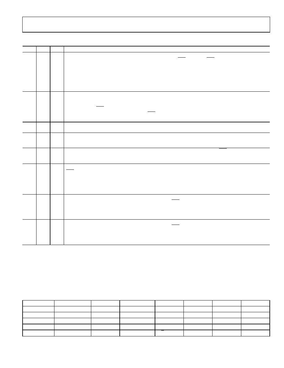
Table 18. Operating Modes
MD2
MD1
MD0
Mode
0
Continuous conversion mode (default). In continuous conversion mode, the ADC continuously performs
conversions and places the result in the data register. The DOUT/RDY pin and the RDY bit in the status register go
low when a conversion is complete. The user can read these conversions by setting the CREAD bit in the commun-
ications register to 1, which enables continuous read. When continuous read is enabled, the conversions are
automatically placed on the DOUT line when SCLK pulses are applied. Alternatively, the user can instruct the ADC to
output each conversion by writing to the communications register. After power-on, a reset, or a reconfiguration of
the ADC, the complete settling time of the filter is required to generate the first valid conversion. Subsequent
conversions are available at the selected output data rate, which is dependent on filter choice.
0
1
Single conversion mode. When single conversion mode is selected, the ADC powers up and performs a single
conversion on the selected channel. The internal clock requires up to 1 ms to power up and settle. The ADC then
performs the conversion, which requires the complete settling time of the filter. The conversion result is placed in
the data register. RDY goes low, and the ADC returns to power-down mode. The conversion remains in the data
register until another conversion is performed. RDY remains active (low) until the data is read or another conversion
is performed.
0
1
0
Idle mode. In idle mode, the ADC filter and modulator are held in a reset state even though the modulator clocks are
still provided.
0
1
Power-down mode. In power-down mode, all AD7192 circuitry, except the bridge power-down switch, is powered
down. The bridge power-down switch remains active because the user may need to power up the sensor prior to
powering up the AD7192 for settling reasons. The external crystal, if selected, remains active.
1
0
Internal zero-scale calibration. An internal short is automatically connected to the input. RDY goes high when the
calibration is initiated and returns low when the calibration is complete. The ADC is placed in idle mode following a
calibration. The measured offset coefficient is placed in the offset register of the selected channel.
1
0
1
Internal full-scale calibration. A full-scale input voltage is automatically connected to the input for this calibration.
RDY goes high when the calibration is initiated and returns low when the calibration is complete. The ADC is placed
in idle mode following a calibration. The measured full-scale coefficient is placed in the full-scale register of the
selected channel. A full-scale calibration is required each time the gain of a channel is changed to minimize the full-
scale error. When AVDD is less than 4.75 V, the CLK_DIV bit must be set when performing the internal full-scale
calibration.
1
0
System zero-scale calibration. The user should connect the system zero-scale input to the channel input pins as
selected by the CH7 to CH0 bits in the configuration register. RDY goes high when the calibration is initiated and
returns low when the calibration is complete. The ADC is placed in idle mode following a calibration. The measured
offset coefficient is placed in the offset register of the selected channel. A system zero-scale calibration is required
each time the gain of a channel is changed.
1
System full-scale calibration. The user should connect the system full-scale input to the channel input pins as
selected by the CH7 to CH0 bits in the configuration register. RDY goes high when the calibration is initiated and
returns low when the calibration is complete. The ADC is placed in idle mode following a calibration. The measured
full-scale coefficient is placed in the full-scale register of the selected channel. A full-scale calibration is required
each time the gain of a channel is changed.
CONFIGURATION REGISTER
(RS2, RS1, RS0 = 0, 1, 0; Power-On/Reset = 0x000117)
The configuration register is a 24-bit register from which data can be read or to which data can be written. This register is used to
configure the ADC for unipolar or bipolar mode, to enable or disable the buffer, to enable or disable the burnout currents, to select the
gain, and to select the analog input channel.
Table 19 outlines the bit designations for the filter register. CON0 through CON23 indicate the bit locations. CON denotes that the bits
are in the configuration register. CON23 denotes the first bit of the data stream. The number in parentheses indicates the power-on/reset
default status of that bit.
CON23
CON22
CON21
CON20
CON19
CON18
CON17
CON16
CHOP(0)
0(0)
REFSEL(0)
0(0)
(0)
CON15
CON14
CON13
CON12
CON11
CON10
CON9
CON8
CH7(0)
CH6(0)
CH5(0)
CH4(0)
CH3(0)
CH2(0)
CH1(0)
CH0(1)
CON7
CON6
CON5
CON4
CON3
CON2
CON1
CON0
BURN(0)
REFDET(0)
0(0)
BUF(1)
U/B (0)
G2(1)
G1(1)
G0(1)
相关PDF资料 |
PDF描述 |
|---|---|
| MS27656T25F24SLC | CONN HSG RCPT 24POS WALL MT SCKT |
| D38999/26JG39PNLC | CONN HSG PLUG 39POS STRGHT PINS |
| AD7783BRU-REEL7 | IC ADC 24BIT 2CH R-R 16-TSSOP |
| D38999/26WE6PALC | CONN HSG PLUG 6POS STRGHT PINS |
| VI-B2H-MY | CONVERTER MOD DC/DC 52V 50W |
相关代理商/技术参数 |
参数描述 |
|---|---|
| AD7193 | 制造商:AD 制造商全称:Analog Devices 功能描述:4-Channel, 4.8 kHz, Ultralow Noise, 24-Bit Sigma-Delta ADC with PGA |
| AD7193BCPZ | 功能描述:IC ADC 24BIT SPI 4.8KHZ 32LFCSP RoHS:是 类别:集成电路 (IC) >> 数据采集 - 模数转换器 系列:- 标准包装:1,000 系列:- 位数:12 采样率(每秒):300k 数据接口:并联 转换器数目:1 功率耗散(最大):75mW 电压电源:单电源 工作温度:0°C ~ 70°C 安装类型:表面贴装 封装/外壳:24-SOIC(0.295",7.50mm 宽) 供应商设备封装:24-SOIC 包装:带卷 (TR) 输入数目和类型:1 个单端,单极;1 个单端,双极 |
| AD7193BCPZ-RL | 功能描述:IC ADC 24BIT SPI 4.8KHZ 32LFCSP RoHS:是 类别:集成电路 (IC) >> 数据采集 - 模数转换器 系列:- 标准包装:1,000 系列:- 位数:16 采样率(每秒):45k 数据接口:串行 转换器数目:2 功率耗散(最大):315mW 电压电源:模拟和数字 工作温度:0°C ~ 70°C 安装类型:表面贴装 封装/外壳:28-SOIC(0.295",7.50mm 宽) 供应商设备封装:28-SOIC W 包装:带卷 (TR) 输入数目和类型:2 个单端,单极 |
| AD7193BCPZ-RL7 | 功能描述:IC ADC 24BIT SPI 4.8KHZ 32LFCSP RoHS:是 类别:集成电路 (IC) >> 数据采集 - 模数转换器 系列:- 标准包装:1,000 系列:- 位数:16 采样率(每秒):45k 数据接口:串行 转换器数目:2 功率耗散(最大):315mW 电压电源:模拟和数字 工作温度:0°C ~ 70°C 安装类型:表面贴装 封装/外壳:28-SOIC(0.295",7.50mm 宽) 供应商设备封装:28-SOIC W 包装:带卷 (TR) 输入数目和类型:2 个单端,单极 |
| AD7193BRUZ | 功能描述:IC ADC 24BIT SPI 4.8K 28-TSSOP RoHS:是 类别:集成电路 (IC) >> 数据采集 - 模数转换器 系列:- 标准包装:1 系列:microPOWER™ 位数:8 采样率(每秒):1M 数据接口:串行,SPI? 转换器数目:1 功率耗散(最大):- 电压电源:模拟和数字 工作温度:-40°C ~ 125°C 安装类型:表面贴装 封装/外壳:24-VFQFN 裸露焊盘 供应商设备封装:24-VQFN 裸露焊盘(4x4) 包装:Digi-Reel® 输入数目和类型:8 个单端,单极 产品目录页面:892 (CN2011-ZH PDF) 其它名称:296-25851-6 |
发布紧急采购,3分钟左右您将得到回复。