参数资料
| 型号: | AD7193BCPZ |
| 厂商: | Analog Devices Inc |
| 文件页数: | 27/57页 |
| 文件大小: | 0K |
| 描述: | IC ADC 24BIT SPI 4.8KHZ 32LFCSP |
| 标准包装: | 1 |
| 位数: | 24 |
| 采样率(每秒): | 4.8k |
| 数据接口: | DSP,MICROWIRE?,QSPI?,串行,SPI? |
| 转换器数目: | 1 |
| 电压电源: | 模拟和数字 |
| 工作温度: | -40°C ~ 105°C |
| 安装类型: | 表面贴装 |
| 封装/外壳: | 32-WFQFN 裸露焊盘,CSP |
| 供应商设备封装: | 32-LFCSP-WQ(5x5) |
| 包装: | 托盘 |
| 输入数目和类型: | 4 个差分,单极;4 个差分,双极;8 个伪差分,单极;8 个伪差分,双极 |
第1页第2页第3页第4页第5页第6页第7页第8页第9页第10页第11页第12页第13页第14页第15页第16页第17页第18页第19页第20页第21页第22页第23页第24页第25页第26页当前第27页第28页第29页第30页第31页第32页第33页第34页第35页第36页第37页第38页第39页第40页第41页第42页第43页第44页第45页第46页第47页第48页第49页第50页第51页第52页第53页第54页第55页第56页第57页
AD7193
Data Sheet
Rev. D | Page 32 of 56
ANALOG INPUT CHANNEL
The AD7193 has four differential/eight pseudo differential analog
input channels that can be buffered or unbuffered. In buffered
mode (the BUF bit in the configuration register is set to 1), the
input channel feeds into a high impedance input stage of the
buffer amplifier. Therefore, the input can tolerate significant
source impedances and is tailored for direct connection to
external resistive type sensors such as strain gages or resistance
temperature detectors (RTDs).
When BUF = 0, the part operates in unbuffered mode. This
results in a higher analog input current. Note that this unbuffered
input path provides a dynamic load to the driving source.
Therefore, resistor/capacitor combinations on the input pins
can cause gain errors, depending on the output impedance of
the source that is driving the ADC input. Table 26 shows the
allowable external resistance/capacitance values for unbuffered
mode at a gain of 1 such that no gain error at the 20-bit level is
introduced.
Table 26. External RC Combination for No 20-Bit Gain Error
C (pF)
R ()
50
1.4 k
100
850
500
300
1000
230
5000
30
The absolute input voltage range in buffered mode is restricted
to a range between AGND + 250 mV and AVDD 250 mV. Care
must be taken in setting up the common-mode voltage to not
exceed these limits; otherwise, linearity and noise performance
degrade.
The absolute input voltage in unbuffered mode includes the
range between AGND 50 mV and AVDD + 50 mV. The
negative absolute input voltage limit allows the possibility of
monitoring small true bipolar signals with respect to AGND.
PROGRAMMABLE GAIN ARRAY (PGA)
When the gain stage is enabled, the output from the buffer is
applied to the input of the PGA. The presence of the PGA means
that signals of small amplitude can be gained within the AD7193
and still maintain excellent noise performance. For example, when
the gain is set to 128, the rms noise is 11 nV, typically, when the
output data rate is 4.7 Hz, which is equivalent to 22.7 bits of
effective resolution or 20 bits of noise free resolution.
The AD7193 can be programmed to have a gain of 1, 8, 16, 32,
64, or 128 by using Bit G2 to Bit G0 in the configuration register.
Therefore, with an external 2.5 V reference, the unipolar ranges
are from 0 mV to 19.53 mV to 0 V to 2.5 V, and the bipolar ranges
are from ±19.53 mV to ±2.5 V.
The analog input range must be limited to ±(AVDD 1.25 V)/gain
because the PGA requires some headroom. Therefore, if VREF =
AVDD = 5 V, the maximum analog input that can be applied to the
AD7193 is 0 V to 3.75 V/gain in unipolar mode or ±3.75 V/gain
in bipolar mode.
REFERENCE
The ADC has a fully differential input capability for the refer-
ence channel. In addition, the user has the option of selecting
one of two external reference options (REFIN1(±) or REFIN2(±)).
The reference source for the AD7193 is selected using the REFSEL
bit in the configuration register. The REFIN2(±) pins are dual
purpose: they can function as two general-purpose output pins
or as reference pins. When the REFSEL bit is set to 1, these pins
automatically function as reference pins.
The common-mode range for these differential inputs is from
AGND to AVDD. The reference voltage REFIN (REFINx(+)
REFINx()) is AVDD nominal, but the AD7193 is functional
with reference voltages from 1 V to AVDD. In applications where
the excitation (voltage or current) for the transducer on the
analog input also drives the reference voltage for the part, the
effect of the low frequency noise in the excitation source is removed
because the application is ratiometric. If the AD7193 is used in a
nonratiometric application, a low noise reference should be used.
The reference input is unbuffered; therefore, excessive RC
source impedances introduce gain errors. RC values similar to
those in Table 26 are recommended for the reference inputs.
Deriving the reference input voltage from an external resistor
means that the reference input sees significant external source
impedance. External decoupling on the REFINx pins is not
recommended in this type of circuit configuration. Conversely,
if large decoupling capacitors are used on the reference inputs,
there should be no resistors in series with the reference inputs.
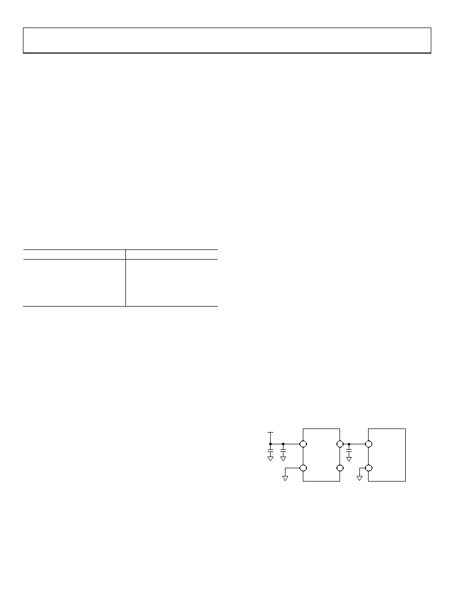
Recommended 2.5 V reference voltage sources for the AD7193
These references tolerate decoupling capacitors on REFINx(+)
without introducing gain errors in the system. Figure 23 shows the
recommended connections between the ADR421 and the AD7193.
4
2
0.1F
AVDD
ADR421
AD7193
VIN
GND
REFINx(+)
REFINx(–)
VOUT
TRIM
10F
4.7F
6
5
08367-
124
Figure 23. ADR421 to AD7193 Connections
相关PDF资料 |
PDF描述 |
|---|---|
| AD7194BCPZ | IC ADC 24BIT SPI 4.8K 32-LFCSP |
| AD7195BCPZ-RL7 | IC AFE 24BIT 4.8K 32LFSP |
| AD7225BQ | IC DAC 8BIT QUAD W/AMP 24-CDIP |
| AD7226BQ | IC DAC 8BIT QUAD W/AMP 20-CDIP |
| AD7228CQ | IC DAC 8BIT OCTAL W/AMP 24-CDIP |
相关代理商/技术参数 |
参数描述 |
|---|---|
| AD7193BCPZ-RL | 功能描述:IC ADC 24BIT SPI 4.8KHZ 32LFCSP RoHS:是 类别:集成电路 (IC) >> 数据采集 - 模数转换器 系列:- 标准包装:1,000 系列:- 位数:16 采样率(每秒):45k 数据接口:串行 转换器数目:2 功率耗散(最大):315mW 电压电源:模拟和数字 工作温度:0°C ~ 70°C 安装类型:表面贴装 封装/外壳:28-SOIC(0.295",7.50mm 宽) 供应商设备封装:28-SOIC W 包装:带卷 (TR) 输入数目和类型:2 个单端,单极 |
| AD7193BCPZ-RL7 | 功能描述:IC ADC 24BIT SPI 4.8KHZ 32LFCSP RoHS:是 类别:集成电路 (IC) >> 数据采集 - 模数转换器 系列:- 标准包装:1,000 系列:- 位数:16 采样率(每秒):45k 数据接口:串行 转换器数目:2 功率耗散(最大):315mW 电压电源:模拟和数字 工作温度:0°C ~ 70°C 安装类型:表面贴装 封装/外壳:28-SOIC(0.295",7.50mm 宽) 供应商设备封装:28-SOIC W 包装:带卷 (TR) 输入数目和类型:2 个单端,单极 |
| AD7193BRUZ | 功能描述:IC ADC 24BIT SPI 4.8K 28-TSSOP RoHS:是 类别:集成电路 (IC) >> 数据采集 - 模数转换器 系列:- 标准包装:1 系列:microPOWER™ 位数:8 采样率(每秒):1M 数据接口:串行,SPI? 转换器数目:1 功率耗散(最大):- 电压电源:模拟和数字 工作温度:-40°C ~ 125°C 安装类型:表面贴装 封装/外壳:24-VFQFN 裸露焊盘 供应商设备封装:24-VQFN 裸露焊盘(4x4) 包装:Digi-Reel® 输入数目和类型:8 个单端,单极 产品目录页面:892 (CN2011-ZH PDF) 其它名称:296-25851-6 |
| AD7193BRUZ | 制造商:Analog Devices 功能描述:IC ADC 24BIT 4.8KHZ TSSOP-28 |
| AD7193BRUZ-REEL | 功能描述:IC ADC 24BIT SPI 4.8KHZ 28TSSOP RoHS:是 类别:集成电路 (IC) >> 数据采集 - 模数转换器 系列:- 标准包装:1,000 系列:- 位数:16 采样率(每秒):45k 数据接口:串行 转换器数目:2 功率耗散(最大):315mW 电压电源:模拟和数字 工作温度:0°C ~ 70°C 安装类型:表面贴装 封装/外壳:28-SOIC(0.295",7.50mm 宽) 供应商设备封装:28-SOIC W 包装:带卷 (TR) 输入数目和类型:2 个单端,单极 |
发布紧急采购,3分钟左右您将得到回复。