参数资料
| 型号: | AD7193BCPZ |
| 厂商: | Analog Devices Inc |
| 文件页数: | 6/57页 |
| 文件大小: | 0K |
| 描述: | IC ADC 24BIT SPI 4.8KHZ 32LFCSP |
| 标准包装: | 1 |
| 位数: | 24 |
| 采样率(每秒): | 4.8k |
| 数据接口: | DSP,MICROWIRE?,QSPI?,串行,SPI? |
| 转换器数目: | 1 |
| 电压电源: | 模拟和数字 |
| 工作温度: | -40°C ~ 105°C |
| 安装类型: | 表面贴装 |
| 封装/外壳: | 32-WFQFN 裸露焊盘,CSP |
| 供应商设备封装: | 32-LFCSP-WQ(5x5) |
| 包装: | 托盘 |
| 输入数目和类型: | 4 个差分,单极;4 个差分,双极;8 个伪差分,单极;8 个伪差分,双极 |
第1页第2页第3页第4页第5页当前第6页第7页第8页第9页第10页第11页第12页第13页第14页第15页第16页第17页第18页第19页第20页第21页第22页第23页第24页第25页第26页第27页第28页第29页第30页第31页第32页第33页第34页第35页第36页第37页第38页第39页第40页第41页第42页第43页第44页第45页第46页第47页第48页第49页第50页第51页第52页第53页第54页第55页第56页第57页
Data Sheet
AD7193
Rev. D | Page 13 of 56
08
36
7-
0
65
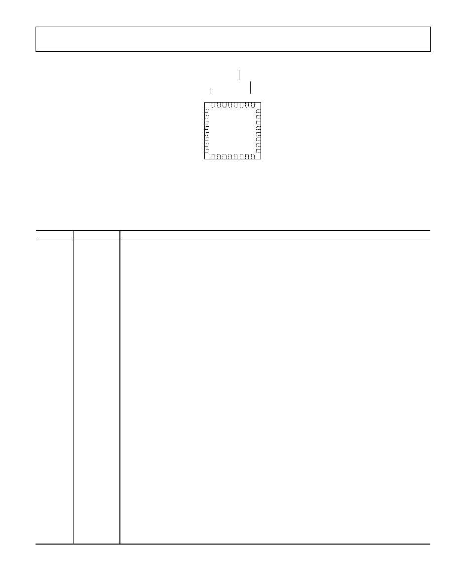
NOTES
1. NC = NO CONNECT.
2. CONNECT EXPOSED PAD TO AGND.
24 DVDD
23 AVDD
22 DGND
21 AGND
20 BPDSW
19 NC
18 REFIN1(–)
17 REFIN1(+)
1
2
3
4
5
6
7
8
P3
P2
P1/REFIN2(+)
P0/REFIN2(–)
NC
AINCOM
9
10
11
12
13
14
15
16
AI
N1
AI
N2
AI
N3
AI
N4
AI
N5
AI
N6
AI
N7
AI
N8
32
31
30
29
28
27
26
25
CS
SC
L
K
MC
L
K
2
MC
L
K
1
DI
N
DO
UT
/RD
Y
NC
SY
N
C
TOP VIEW
(Not to Scale)
AD7193
Figure 6. 32-Lead LFCSP Pin Configuration
Table 6. 32-Lead LFCSP Pin Function Descriptions
Pin No.
Mnemonic
Description
1
P3
Digital Output Pin. This pin can function as a general-purpose output bit referenced between AVDD and
AGND.
2
P2
Digital Output Pin. This pin can function as a general-purpose output bit referenced between AVDD and
AGND.
3
P1/REFIN2(+)
Digital Output Pin/Positive Reference Input. This pin functions as a general-purpose output bit referenced
between AVDD and AGND. When the REFSEL bit in the configuration register = 1, this pin functions as
REFIN2(+). An external reference can be applied between REFIN2(+) and REFIN2(). REFIN2(+) can lie
anywhere between AVDD and AGND + 1 V. The nominal reference voltage, (REFIN2(+) REFIN2()), is AVDD, but
the part functions with a reference from 1 V to AVDD.
4
P0/REFIN2()
Digital Output Pin/Negative Reference Input. This pin functions as a general-purpose output bit referenced
between AVDD and AGND. When the REFSEL bit in the configuration register = 1, this pin functions as
REFIN2(). This reference input can lie anywhere between AGND and AVDD 1 V.
5, 6, 7, 19,
26
NC
No Connect. Tie these pins to AGND.
8
AINCOM
Analog Input AIN1 to Analog Input AIN8 are referenced to this input when configured for pseudo differential
operation.
9
AIN1
Analog Input. This pin can be configured as the positive input of a fully differential input pair when used with
AIN2 or as a pseudo differential input when used with AINCOM.
10
AIN2
Analog Input. This pin can be configured as the negative input of a fully differential input pair when used
with AIN1 or as a pseudo differential input when used with AINCOM.
11
AIN3
Analog Input. This pin can be configured as the positive input of a fully differential input pair when used with
AIN4 or as a pseudo differential input when used with AINCOM.
12
AIN4
Analog Input. This pin can be configured as the negative input of a fully differential input pair when used
with AIN3 or as a pseudo differential input when used with AINCOM.
13
AIN5
Analog Input. This pin can be configured as the positive input of a fully differential input pair when used with
AIN6 or as a pseudo differential input when used with AINCOM.
14
AIN6
Analog Input. This pin can be configured as the negative input of a fully differential input pair when used
with AIN5 or as a pseudo differential input when used with AINCOM.
15
AIN7
Analog Input. This pin can be configured as the positive input of a fully differential input pair when used with
AIN8 or as a pseudo differential input when used with AINCOM.
16
AIN8
Analog Input. This pin can be configured as the negative input of a fully differential input pair when used
with AIN7 or as a pseudo differential input when used with AINCOM.
17
REFIN1(+)
Positive Reference Input. An external reference can be applied between REFIN1(+) and REFIN1(). REFIN1(+)
can lie anywhere between AVDD and AGND + 1 V. The nominal reference voltage, (REFIN1(+) REFIN1()), is
AVDD, but the part functions with a reference from 1 V to AVDD.
18
REFIN1()
Negative Reference Input. This reference input can lie anywhere between AGND and AVDD 1 V.
20
BPDSW
Bridge Power-Down Switch to AGND.
相关PDF资料 |
PDF描述 |
|---|---|
| AD7194BCPZ | IC ADC 24BIT SPI 4.8K 32-LFCSP |
| AD7195BCPZ-RL7 | IC AFE 24BIT 4.8K 32LFSP |
| AD7225BQ | IC DAC 8BIT QUAD W/AMP 24-CDIP |
| AD7226BQ | IC DAC 8BIT QUAD W/AMP 20-CDIP |
| AD7228CQ | IC DAC 8BIT OCTAL W/AMP 24-CDIP |
相关代理商/技术参数 |
参数描述 |
|---|---|
| AD7193BCPZ-RL | 功能描述:IC ADC 24BIT SPI 4.8KHZ 32LFCSP RoHS:是 类别:集成电路 (IC) >> 数据采集 - 模数转换器 系列:- 标准包装:1,000 系列:- 位数:16 采样率(每秒):45k 数据接口:串行 转换器数目:2 功率耗散(最大):315mW 电压电源:模拟和数字 工作温度:0°C ~ 70°C 安装类型:表面贴装 封装/外壳:28-SOIC(0.295",7.50mm 宽) 供应商设备封装:28-SOIC W 包装:带卷 (TR) 输入数目和类型:2 个单端,单极 |
| AD7193BCPZ-RL7 | 功能描述:IC ADC 24BIT SPI 4.8KHZ 32LFCSP RoHS:是 类别:集成电路 (IC) >> 数据采集 - 模数转换器 系列:- 标准包装:1,000 系列:- 位数:16 采样率(每秒):45k 数据接口:串行 转换器数目:2 功率耗散(最大):315mW 电压电源:模拟和数字 工作温度:0°C ~ 70°C 安装类型:表面贴装 封装/外壳:28-SOIC(0.295",7.50mm 宽) 供应商设备封装:28-SOIC W 包装:带卷 (TR) 输入数目和类型:2 个单端,单极 |
| AD7193BRUZ | 功能描述:IC ADC 24BIT SPI 4.8K 28-TSSOP RoHS:是 类别:集成电路 (IC) >> 数据采集 - 模数转换器 系列:- 标准包装:1 系列:microPOWER™ 位数:8 采样率(每秒):1M 数据接口:串行,SPI? 转换器数目:1 功率耗散(最大):- 电压电源:模拟和数字 工作温度:-40°C ~ 125°C 安装类型:表面贴装 封装/外壳:24-VFQFN 裸露焊盘 供应商设备封装:24-VQFN 裸露焊盘(4x4) 包装:Digi-Reel® 输入数目和类型:8 个单端,单极 产品目录页面:892 (CN2011-ZH PDF) 其它名称:296-25851-6 |
| AD7193BRUZ | 制造商:Analog Devices 功能描述:IC ADC 24BIT 4.8KHZ TSSOP-28 |
| AD7193BRUZ-REEL | 功能描述:IC ADC 24BIT SPI 4.8KHZ 28TSSOP RoHS:是 类别:集成电路 (IC) >> 数据采集 - 模数转换器 系列:- 标准包装:1,000 系列:- 位数:16 采样率(每秒):45k 数据接口:串行 转换器数目:2 功率耗散(最大):315mW 电压电源:模拟和数字 工作温度:0°C ~ 70°C 安装类型:表面贴装 封装/外壳:28-SOIC(0.295",7.50mm 宽) 供应商设备封装:28-SOIC W 包装:带卷 (TR) 输入数目和类型:2 个单端,单极 |
发布紧急采购,3分钟左右您将得到回复。