参数资料
| 型号: | AD7193BCPZ |
| 厂商: | Analog Devices Inc |
| 文件页数: | 37/57页 |
| 文件大小: | 0K |
| 描述: | IC ADC 24BIT SPI 4.8KHZ 32LFCSP |
| 标准包装: | 1 |
| 位数: | 24 |
| 采样率(每秒): | 4.8k |
| 数据接口: | DSP,MICROWIRE?,QSPI?,串行,SPI? |
| 转换器数目: | 1 |
| 电压电源: | 模拟和数字 |
| 工作温度: | -40°C ~ 105°C |
| 安装类型: | 表面贴装 |
| 封装/外壳: | 32-WFQFN 裸露焊盘,CSP |
| 供应商设备封装: | 32-LFCSP-WQ(5x5) |
| 包装: | 托盘 |
| 输入数目和类型: | 4 个差分,单极;4 个差分,双极;8 个伪差分,单极;8 个伪差分,双极 |
第1页第2页第3页第4页第5页第6页第7页第8页第9页第10页第11页第12页第13页第14页第15页第16页第17页第18页第19页第20页第21页第22页第23页第24页第25页第26页第27页第28页第29页第30页第31页第32页第33页第34页第35页第36页当前第37页第38页第39页第40页第41页第42页第43页第44页第45页第46页第47页第48页第49页第50页第51页第52页第53页第54页第55页第56页第57页
Data Sheet
AD7193
Rev. D | Page 41 of 56
DIGITAL FILTER
The AD7193 offers a lot of flexibility in the digital filter. The
device has five filter options. The device can be operated with
a sinc3 or sinc4 filter, chop can be enabled or disabled, and zero
latency can be enabled. Finally, an averaging block can be
included after the sinc filter, which gives a fast settling mode.
The option selected affects the output data rate, settling time,
and 50 Hz/60 Hz rejection. The following sections describe
each filter type, indicating the available output data rates for
each filter option. The filter response, along with the settling
time and 50 Hz/60 Hz rejection, is also discussed.
SINC4 FILTER (CHOP DISABLED)
When the AD7193 is powered up, the sinc4 filter is selected by
default and chop is disabled. This filter gives excellent noise
performance over the complete range of output data rates. It
also gives the best 50 Hz/60 Hz rejection, but it has a long
settling time.
SINC3/SINC4
POST FILTER
MODULATOR
ADC
CHOP
083
67
-024
Figure 28. Sinc4 Filter (Chop Disabled)
Sinc4 Output Data Rate/Settling Time
The output data rate (the rate at which conversions are available
on a single channel when the ADC is continuously converting)
is equal to
fADC = fCLK/(1024 × FS[9:0])
where:
fADC is the output data rate.
fCLK is the master clock (4.92 MHz nominal).
FS[9:0] is the decimal equivalent of Bit FS9 to Bit FS0 in the
mode register.
The output data rate can be programmed from 4.7 Hz to
4800 Hz; that is, FS[9:0] can have a value from 1 to 1023.
The settling time for the sinc4 filter is equal to
tSETTLE = 4/fADC
When a channel change occurs, the modulator and filter are
reset. The settling time is allowed to generate the first conver-
sion after the channel change. Subsequent conversions on this
channel occur at 1/fADC.
CHANNEL
CONVERSIONS
CHANNEL A
CH A CH A CH A
CH B CH B CH B
CHANNEL B
1/
fADC
0
83
67
-0
25
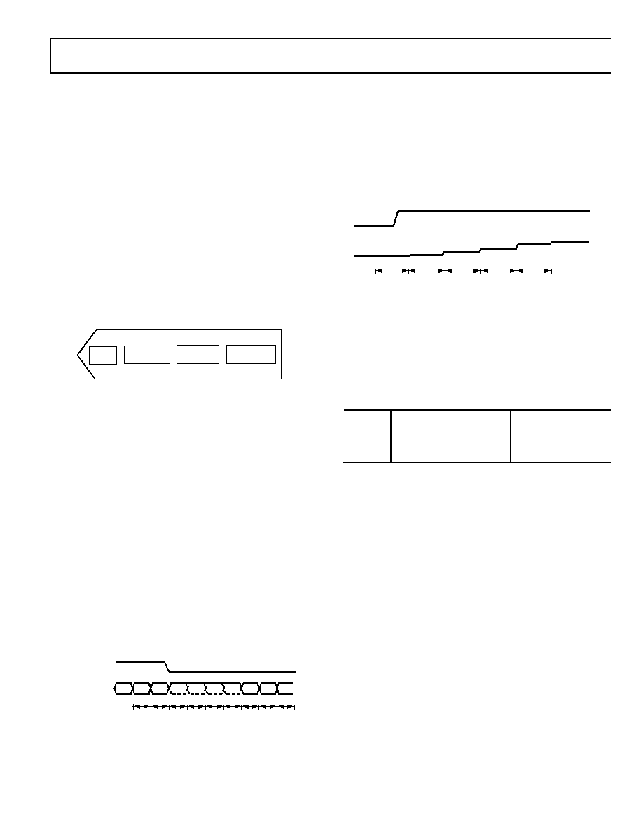
Figure 29. Sinc4 Channel Change
When conversions are performed on a single channel and a step
change occurs, the ADC does not detect the change in analog
input. Therefore, it continues to output conversions at the pro-
grammed output data rate. However, it is at least four conversions
later before the output data accurately reflect the analog input.
If the step change occurs while the ADC is processing a conver-
sion, then the ADC takes five conversions after the step change
to generate a fully settled result.
1/
fADC
ANALOG
INPUT
ADC
OUTPUT
FULLY
SETTLED
08
36
7-
02
6
Figure 30. Asynchronous Step Change in Analog Input
The 3 dB frequency for the sinc4 filter is equal to
f3dB = 0.23 × fADC
Table 28 gives some examples of the relationship between the
values in Bits FS[9:0] and the corresponding output data rate
and settling time.
Table 28. Examples of Output Data Rates and the
Corresponding Settling Time
FS[9:0]
Output Data Rate (Hz)
Settling Time (ms)
480
10
400
96
50
80
60
66.6
Sinc4 Zero Latency
Zero latency is enabled by setting the single bit (Bit 11) in the
mode register to 1. With zero latency, the complete settling time
is allowed for each conversion. Therefore, the conversion time
when converting on a single channel or when converting on
several channels is constant. The user does not need to consider
the effects of channel changes on the output data rate. When the
channel sequencer is enabled, the AD7193 automatically
operates in zero latency mode.
The output data rate equals
fADC = 1/tSETTLE = fCLK/(4 × 1024 × FS[9:0])
where:
fADC is the output data rate.
fCLK is the master clock (4.92 MHz nominal).
FS[9:0] is the decimal equivalent of Bit FS9 to Bit FS0 in the
mode register.
相关PDF资料 |
PDF描述 |
|---|---|
| AD7194BCPZ | IC ADC 24BIT SPI 4.8K 32-LFCSP |
| AD7195BCPZ-RL7 | IC AFE 24BIT 4.8K 32LFSP |
| AD7225BQ | IC DAC 8BIT QUAD W/AMP 24-CDIP |
| AD7226BQ | IC DAC 8BIT QUAD W/AMP 20-CDIP |
| AD7228CQ | IC DAC 8BIT OCTAL W/AMP 24-CDIP |
相关代理商/技术参数 |
参数描述 |
|---|---|
| AD7193BCPZ-RL | 功能描述:IC ADC 24BIT SPI 4.8KHZ 32LFCSP RoHS:是 类别:集成电路 (IC) >> 数据采集 - 模数转换器 系列:- 标准包装:1,000 系列:- 位数:16 采样率(每秒):45k 数据接口:串行 转换器数目:2 功率耗散(最大):315mW 电压电源:模拟和数字 工作温度:0°C ~ 70°C 安装类型:表面贴装 封装/外壳:28-SOIC(0.295",7.50mm 宽) 供应商设备封装:28-SOIC W 包装:带卷 (TR) 输入数目和类型:2 个单端,单极 |
| AD7193BCPZ-RL7 | 功能描述:IC ADC 24BIT SPI 4.8KHZ 32LFCSP RoHS:是 类别:集成电路 (IC) >> 数据采集 - 模数转换器 系列:- 标准包装:1,000 系列:- 位数:16 采样率(每秒):45k 数据接口:串行 转换器数目:2 功率耗散(最大):315mW 电压电源:模拟和数字 工作温度:0°C ~ 70°C 安装类型:表面贴装 封装/外壳:28-SOIC(0.295",7.50mm 宽) 供应商设备封装:28-SOIC W 包装:带卷 (TR) 输入数目和类型:2 个单端,单极 |
| AD7193BRUZ | 功能描述:IC ADC 24BIT SPI 4.8K 28-TSSOP RoHS:是 类别:集成电路 (IC) >> 数据采集 - 模数转换器 系列:- 标准包装:1 系列:microPOWER™ 位数:8 采样率(每秒):1M 数据接口:串行,SPI? 转换器数目:1 功率耗散(最大):- 电压电源:模拟和数字 工作温度:-40°C ~ 125°C 安装类型:表面贴装 封装/外壳:24-VFQFN 裸露焊盘 供应商设备封装:24-VQFN 裸露焊盘(4x4) 包装:Digi-Reel® 输入数目和类型:8 个单端,单极 产品目录页面:892 (CN2011-ZH PDF) 其它名称:296-25851-6 |
| AD7193BRUZ | 制造商:Analog Devices 功能描述:IC ADC 24BIT 4.8KHZ TSSOP-28 |
| AD7193BRUZ-REEL | 功能描述:IC ADC 24BIT SPI 4.8KHZ 28TSSOP RoHS:是 类别:集成电路 (IC) >> 数据采集 - 模数转换器 系列:- 标准包装:1,000 系列:- 位数:16 采样率(每秒):45k 数据接口:串行 转换器数目:2 功率耗散(最大):315mW 电压电源:模拟和数字 工作温度:0°C ~ 70°C 安装类型:表面贴装 封装/外壳:28-SOIC(0.295",7.50mm 宽) 供应商设备封装:28-SOIC W 包装:带卷 (TR) 输入数目和类型:2 个单端,单极 |
发布紧急采购,3分钟左右您将得到回复。