参数资料
| 型号: | AD7194BCPZ |
| 厂商: | Analog Devices Inc |
| 文件页数: | 15/57页 |
| 文件大小: | 0K |
| 描述: | IC ADC 24BIT SPI 4.8K 32-LFCSP |
| 产品培训模块: | Weigh Scale Introduction |
| 标准包装: | 1 |
| 位数: | 24 |
| 采样率(每秒): | 4.8k |
| 数据接口: | DSP,MICROWIRE?,QSPI?,串行,SPI? |
| 转换器数目: | 1 |
| 电压电源: | 模拟和数字 |
| 工作温度: | -40°C ~ 105°C |
| 安装类型: | 表面贴装 |
| 封装/外壳: | 32-WFQFN 裸露焊盘,CSP |
| 供应商设备封装: | 32-LFCSP-WQ(5x5) |
| 包装: | 管件 |
| 输入数目和类型: | 8 个差分,单极;8 个差分,双极;16 个伪差分,单极;16 伪差分,双极 |
| 产品目录页面: | 777 (CN2011-ZH PDF) |
| 其它名称: | AD7194BRUZ AD7194BRUZ-ND |
第1页第2页第3页第4页第5页第6页第7页第8页第9页第10页第11页第12页第13页第14页当前第15页第16页第17页第18页第19页第20页第21页第22页第23页第24页第25页第26页第27页第28页第29页第30页第31页第32页第33页第34页第35页第36页第37页第38页第39页第40页第41页第42页第43页第44页第45页第46页第47页第48页第49页第50页第51页第52页第53页第54页第55页第56页第57页
Data Sheet
AD7194
Rev. A | Page 21 of 56
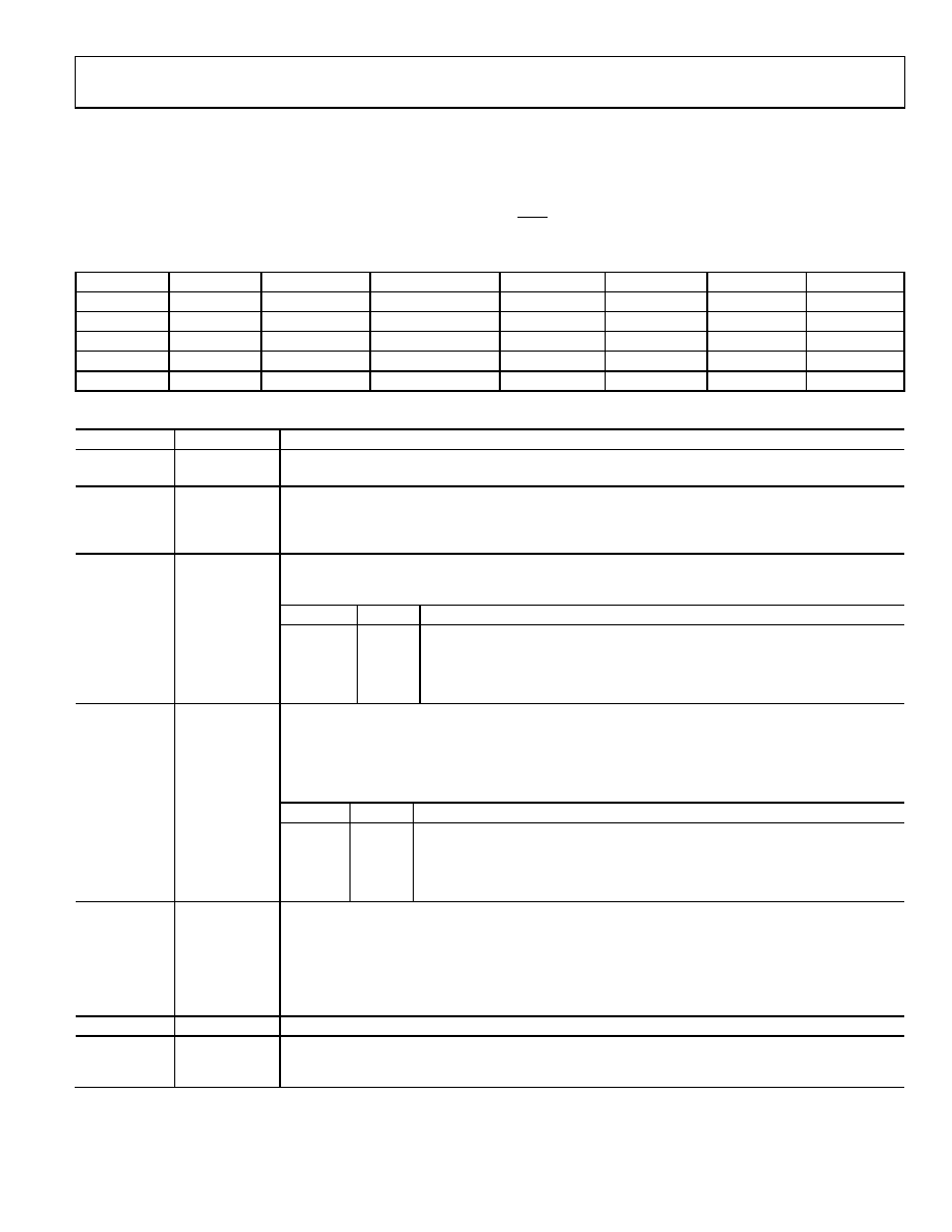
MODE REGISTER
RS2, RS1, RS0 = 001; Power-On/Reset = 0x080060
The mode register is a 24-bit register from which data can be
read or to which data can be written. This register is used to
select the operating mode, the output data rate, and the clock
source. Table 19 outlines the bit designations for the mode
register. MR0 through MR23 indicate the bit locations, MR
denoting that the bits are in the mode register. MR23 denotes
the first bit of the data stream. The number in parentheses
indicates the power-on/reset default status of that bit. Any write
to the mode register resets the modulator and filter and sets the
RDY bit.
MR23
MR22
MR21
MR20
MR19
MR18
MR17
MR16
MD2(0)
MD1(0)
MD0(0)
DAT_STA(0)
CLK1(1)
CLK0(0)
AVG1(0)
AVG0(0)
MR15
MR14
MR13
MR12
MR11
MR10
MR9
MR8
SINC3(0)
0
ENPAR(0)
CLK_DIV(0)
Single(0)
REJ60(0)
FS9(0)
FS8(0)
MR7
MR6
MR5
MR4
MR3
MR2
MR1
MR0
FS7(0)
FS6(1)
FS5(1)
FS4(0)
FS3(0)
FS2(0)
FS1(0)
FS0(0)
Table 19. Mode Register (MR) Bit Designations
Bit Location
Bit Name
Description
MR23 to
MR21
MD2 to MD0
Mode select bits. These bits select the operating mode of the AD7194 (see Table 20).
MR20
DAT_STA
This bit enables the transmission of status register contents after each data register read. When DAT_STA
is set, the contents of the status register are transmitted along with each data register read. This function
is useful when several channels are selected because the status register identifies the channel to which
the data register value corresponds.
MR19, MR18
CLK1, CLK0
These bits select the clock source for the AD7194. Either the on-chip 4.92 MHz clock or an external clock
can be used. The ability to use an external clock allows several AD7194 devices to be synchronized. Also,
50 Hz/60 Hz rejection is improved when an accurate external clock drives the AD7194.
CLK1
CLK0
ADC Clock Source
0
External crystal. The external crystal is connected from MCLK1 to MCLK2.
0
1
External clock. The external clock is applied to the MCLK2 pin.
1
0
Internal 4.92 MHz clock. Pin MCLK2 is tristated.
1
Internal 4.92 MHz clock. The internal clock is available on MCLK2.
MR17, MR16
AVG1, AVG0
Fast settling filter. When this option is selected, the settling time equals one conversion time. In fast
settling mode, a first-order average and decimate block is included after the sinc filter. The data from the
sinc filter is averaged by 2, 8, or 16. The averaging reduces the output data rate for a given FS word;
however, the rms noise improves. The AVG1 and AVG0 bits select the amount of averaging. Fast settling
mode can be used for FS words less than 512 only. When the sinc3 filter is selected, the FS word must be
less than 256 when averaging by 16.
AVG1
AVG0
Average
0
No averaging (fast settling mode disabled)
0
1
Average by 2
1
0
Average by 8
1
Average by 16
MR15
SINC3
Sinc3 filter select bit. When this bit is cleared, the sinc4 filter is used (default value). When this bit is set,
the sinc3 filter is used. The benefit of the sinc3 filter compared to the sinc4 filter is its lower settling time.
For a given output data rate, fADC, the sinc3 filter has a settling time of 3/fADC whereas the sinc4 filter has
a settling time of 4/fADC when chop is disabled. The sinc4 filter, due to its deeper notches, gives better
50 Hz/60 Hz rejection. At low output data rates, both filters give similar rms noise and similar no missing
codes for a given output data rate. At higher output data rates (FS values less than 5), the sinc4 filter gives
better performance than the sinc3 filter for rms noise and no missing codes.
MR14
0
This bit must be programmed with a Logic 0 for correct operation.
MR13
ENPAR
Enable parity bit. When ENPAR is set, parity checking on the data register is enabled. The DAT_STA bit in
the mode register should be set when the parity check is used. When the DAT_STA bit is set, the contents
of the status register are transmitted along with the data for each data register read.
相关PDF资料 |
PDF描述 |
|---|---|
| AD7195BCPZ-RL7 | IC AFE 24BIT 4.8K 32LFSP |
| AD7225BQ | IC DAC 8BIT QUAD W/AMP 24-CDIP |
| AD7226BQ | IC DAC 8BIT QUAD W/AMP 20-CDIP |
| AD7228CQ | IC DAC 8BIT OCTAL W/AMP 24-CDIP |
| AD7233BNZ | IC DAC 12BIT SRL W/AMP 8PDIP |
相关代理商/技术参数 |
参数描述 |
|---|---|
| AD7194BCPZ-REEL | 功能描述:IC ADC 24BIT SPI 4.8KHZ 32LFCSP RoHS:是 类别:集成电路 (IC) >> 数据采集 - 模数转换器 系列:- 标准包装:1,000 系列:- 位数:16 采样率(每秒):45k 数据接口:串行 转换器数目:2 功率耗散(最大):315mW 电压电源:模拟和数字 工作温度:0°C ~ 70°C 安装类型:表面贴装 封装/外壳:28-SOIC(0.295",7.50mm 宽) 供应商设备封装:28-SOIC W 包装:带卷 (TR) 输入数目和类型:2 个单端,单极 |
| AD7194BCPZ-REEL7 | 功能描述:IC ADC 24BIT SPI 4.8KHZ 32LFCSP RoHS:是 类别:集成电路 (IC) >> 数据采集 - 模数转换器 系列:- 标准包装:1,000 系列:- 位数:16 采样率(每秒):45k 数据接口:串行 转换器数目:2 功率耗散(最大):315mW 电压电源:模拟和数字 工作温度:0°C ~ 70°C 安装类型:表面贴装 封装/外壳:28-SOIC(0.295",7.50mm 宽) 供应商设备封装:28-SOIC W 包装:带卷 (TR) 输入数目和类型:2 个单端,单极 |
| AD7195 | 制造商:AD 制造商全称:Analog Devices 功能描述:4.8 kHz, Ultralow Noise, 24-Bit Sigma-Delta ADC with PGA and AC Excitation |
| AD7195BCPZ | 功能描述:IC AFE 24BIT 4.8K 32LFSP RoHS:是 类别:集成电路 (IC) >> 数据采集 - 模拟前端 (AFE) 系列:- 产品培训模块:Lead (SnPb) Finish for COTS Obsolescence Mitigation Program 标准包装:2,500 系列:- 位数:- 通道数:2 功率(瓦特):- 电压 - 电源,模拟:3 V ~ 3.6 V 电压 - 电源,数字:3 V ~ 3.6 V 封装/外壳:32-VFQFN 裸露焊盘 供应商设备封装:32-QFN(5x5) 包装:带卷 (TR) |
| AD7195BCPZ | 制造商:Analog Devices 功能描述:IC ADC 24BIT 4.8KSPS CSP-32 |
发布紧急采购,3分钟左右您将得到回复。