参数资料
| 型号: | AD7195BCPZ-RL7 |
| 厂商: | Analog Devices Inc |
| 文件页数: | 31/45页 |
| 文件大小: | 0K |
| 描述: | IC AFE 24BIT 4.8K 32LFSP |
| 设计资源: | Precision Weigh Scale Design Using AD7195 with Internal PGA and AC Excitation (CN0155) |
| 标准包装: | 1,500 |
| 位数: | 24 |
| 通道数: | 4 |
| 电压 - 电源,模拟: | 4.75 V ~ 5.25 V |
| 电压 - 电源,数字: | 2.7 V ~ 5.25 V |
| 封装/外壳: | 32-WFQFN 裸露焊盘,CSP |
| 供应商设备封装: | 32-LFCSP-WQ(5x5) |
| 包装: | 带卷 (TR) |
第1页第2页第3页第4页第5页第6页第7页第8页第9页第10页第11页第12页第13页第14页第15页第16页第17页第18页第19页第20页第21页第22页第23页第24页第25页第26页第27页第28页第29页第30页当前第31页第32页第33页第34页第35页第36页第37页第38页第39页第40页第41页第42页第43页第44页第45页
AD7195
Rev. 0 | Page 36 of 44
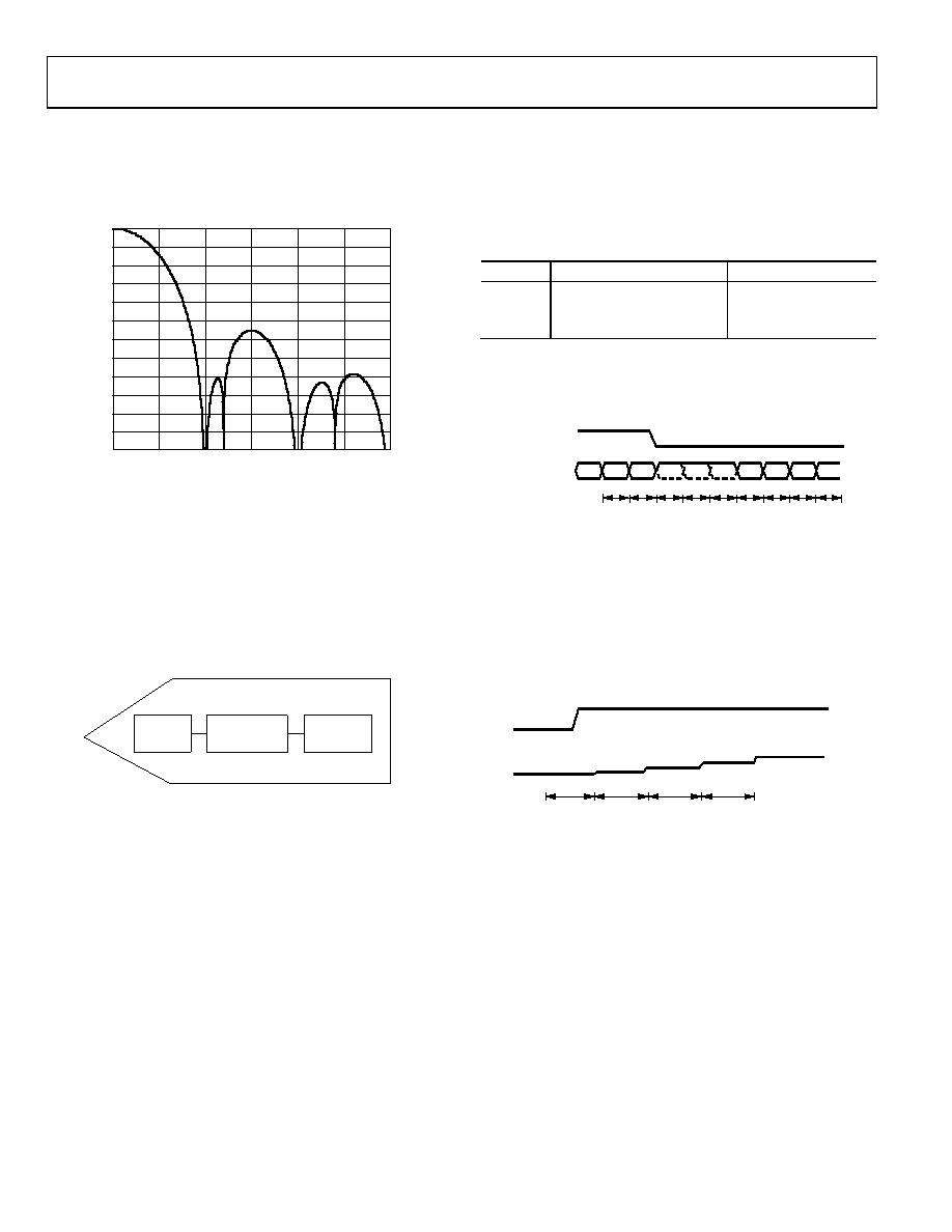
The output data rate is 50 Hz when zero latency is disabled and
12.5 Hz when zero latency is enabled. Figure 31 shows the
frequency response of the sinc4 filter. The filter provides 50 Hz
±1 Hz and 60 Hz ± 1 Hz rejection of 82 dB minimum, assuming
a stable 4.92 MHz master clock.
–120
–110
–100
–90
–80
–70
–60
–50
–40
–30
–20
–10
0
25
50
75
100
125
150
FREQUENCY (Hz)
F
IL
T
E
R
GA
IN
(
d
B
)
08
77
1
-04
4
Figure 31. Sinc4 Filter Response (FS[9:0] = 96, REJ60 = 1)
SINC3 FILTER (CHOP DISABLED)
A sinc3 filter can be used instead of the sinc4 filter. The filter is
selected using the SINC3 bit in the mode register. The sinc3
filter is selected when the SINC3 bit is set to 1.
This filter has good noise performance when operating with
output data rates up to 1 kHz. It has moderate settling time and
moderate 50 Hz/60 Hz (±1 Hz) rejection.
0
87
71
-034
SINC3/SINC4
MODULATOR
ADC
CHOP
Figure 32. Sinc3 Filter (Chop Disabled)
Sinc3 Output Data Rate and Settling Time
The output data rate (the rate at which conversions are available
on a single channel when the ADC is continuously converting)
is equal to
fADC = fCLK/(1024 × FS[9:0])
where:
fADC is the output data rate.
fCLK is the master clock (4.92 MHz nominal).
FS[9:0] is the decimal equivalent of Bit FS9 to Bit FS0 in the
mode register.
The output data rate can be programmed from 4.7 Hz to
4800 Hz; that is, FS[9:0] can have a value from 1 to 1023.
The settling time is equal to
tSETTLE = 3/fADC
The 3 dB frequency is equal to
f3dB = 0.272 × fADC
Table 31 gives some examples of FS settings and the corres-
ponding output data rates and settling times.
Table 31. Examples of Output Data Rates and the
Corresponding Settling Time
FS[9:0]
Output Data Rate (Hz)
Settling Time (ms)
480
10
300
96
50
60
80
60
50
When a channel change occurs, the modulator and filter reset.
The complete settling time is allowed to generate the first
conversion after the channel change (see Figure 33). Subsequent
conversions on this channel are available at 1/fADC.
CHANNEL
CONVERSIONS
CHANNEL A
CH A
CH B
CHANNEL B
1/
fADC
0
87
71
-0
45
Figure 33. Sinc3 Channel Change
When conversions are performed on a single channel and a step
change occurs, the ADC does not detect the change in analog
input. Therefore, it continues to output conversions at the program-
med output data rate. However, it is at least three conversions later
before the output data accurately reflects the analog input. If the
step change occurs while the ADC is processing a conversion, the
ADC takes four conversions after the step change to generate a fully
settled result.
1/
fADC
ANALOG
INPUT
ADC
OUTPUT
FULLY
SETTLED
0
877
1-
0
46
Figure 34. Asynchronous Step Change in Analog Input
Sinc3 Zero Latency
Zero latency is enabled by setting the single bit (Bit 11) in the
mode register to 1. With zero latency, the complete settling time
is allowed for each conversion. Therefore, the conversion time
when converting on a single channel or when converting on
several channels is constant. The user does not need to consider
the effects of channel changes on the output data rate.
相关PDF资料 |
PDF描述 |
|---|---|
| AD7225BQ | IC DAC 8BIT QUAD W/AMP 24-CDIP |
| AD7226BQ | IC DAC 8BIT QUAD W/AMP 20-CDIP |
| AD7228CQ | IC DAC 8BIT OCTAL W/AMP 24-CDIP |
| AD7233BNZ | IC DAC 12BIT SRL W/AMP 8PDIP |
| AD7243BQ | IC DAC 12BIT W/AMP W/REF 16-CDIP |
相关代理商/技术参数 |
参数描述 |
|---|---|
| AD71L | 制造商:Johnson Components 功能描述:ADAPT - Bulk |
| AD72 | 制造商:Distributed By MCM 功能描述:REFRIGERATR DOOR GASKET DIRECT |
| AD720 | 制造商:AD 制造商全称:Analog Devices 功能描述:RGB to NTSC/PAL Encoders |
| AD720-00E | 功能描述:SENSOR MAG SW 28G STANDRD 8-MSOP 制造商:nve corp/sensor products 系列:AD 包装:管件 零件状态:有效 功能:全极开关 技术:霍尔效应 极化:任意一种 感应范围:±3.4mT 跳闸,±1.4mT 释放 测试条件:-40°C ~ 125°C 电压 - 电源:4.5 V ~ 30 V 电流 - 电源(最大值):4.5mA 电流 - 输出(最大值):20mA 输出类型:开路集电极 特性:- 工作温度:-40°C ~ 125°C(TA) 封装/外壳:8-TSSOP,8-MSOP(0.118",3.00mm 宽) 供应商器件封装:8-MSOP 标准包装:1,000 |
| AD720-02E | 功能描述:SENSOR MAG SW 28G STANDARD 8SOIC 制造商:nve corp/sensor products 系列:AD 包装:管件 零件状态:有效 功能:全极开关 技术:霍尔效应 极化:任意一种 感应范围:±3.4mT 跳闸,±1.4mT 释放 测试条件:-40°C ~ 125°C 电压 - 电源:4.5 V ~ 30 V 电流 - 电源(最大值):4.5mA 电流 - 输出(最大值):20mA 输出类型:开路集电极 特性:- 工作温度:-40°C ~ 125°C(TA) 封装/外壳:8-SOIC(0.154",3.90mm 宽) 供应商器件封装:8-SOIC 标准包装:1,000 |
发布紧急采购,3分钟左右您将得到回复。