参数资料
| 型号: | AD7195BCPZ-RL7 |
| 厂商: | Analog Devices Inc |
| 文件页数: | 43/45页 |
| 文件大小: | 0K |
| 描述: | IC AFE 24BIT 4.8K 32LFSP |
| 设计资源: | Precision Weigh Scale Design Using AD7195 with Internal PGA and AC Excitation (CN0155) |
| 标准包装: | 1,500 |
| 位数: | 24 |
| 通道数: | 4 |
| 电压 - 电源,模拟: | 4.75 V ~ 5.25 V |
| 电压 - 电源,数字: | 2.7 V ~ 5.25 V |
| 封装/外壳: | 32-WFQFN 裸露焊盘,CSP |
| 供应商设备封装: | 32-LFCSP-WQ(5x5) |
| 包装: | 带卷 (TR) |
第1页第2页第3页第4页第5页第6页第7页第8页第9页第10页第11页第12页第13页第14页第15页第16页第17页第18页第19页第20页第21页第22页第23页第24页第25页第26页第27页第28页第29页第30页第31页第32页第33页第34页第35页第36页第37页第38页第39页第40页第41页第42页当前第43页第44页第45页
AD7195
Rev. 0 | Page 6 of 44
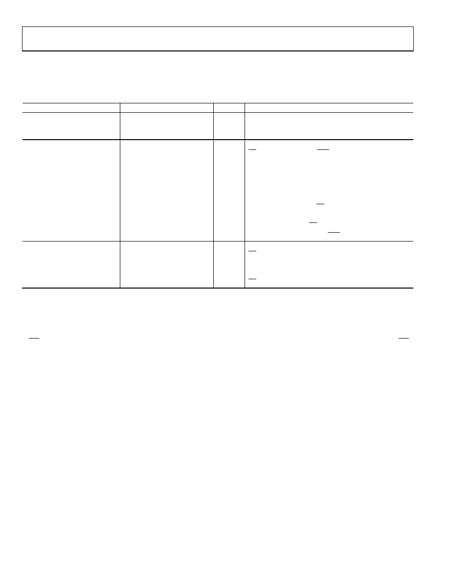
TIMING CHARACTERISTICS
AVDD = 4.75 V to 5.25 V, DVDD = 2.7 V to 5.25 V, AGND = DGND = 0 V, Input Logic 0 = 0 V, Input Logic 1 = DVDD, unless
otherwise noted.
Table 2.
Parameter
Limit at TMIN, TMAX (B Version)
Unit
Conditions/Comments1, 2
READ AND WRITE OPERATIONS
t3
100
ns min
SCLK high pulse width
t4
100
ns min
SCLK low pulse width
READ OPERATION
t1
0
ns min
CS falling edge to DOUT/RDY active time
60
ns max
DVDD = 4.75 V to 5.25 V
80
ns max
DVDD = 2.7 V to 3.6 V
t23
0
ns min
SCLK active edge to data valid delay4
60
ns max
DVDD = 4.75 V to 5.25 V
80
ns max
DVDD = 2.7 V to 3.6 V
t55, 6
10
ns min
Bus relinquish time after CS inactive edge
80
ns max
t6
0
ns min
SCLK inactive edge to CS inactive edge
t7
10
ns min
SCLK inactive edge to DOUT/RDY high
WRITE OPERATION
t8
0
ns min
CS falling edge to SCLK active edge setup time4
t9
30
ns min
Data valid to SCLK edge setup time
t10
25
ns min
Data valid to SCLK edge hold time
t11
0
ns min
CS rising edge to SCLK edge hold time
1 Sample tested during initial release to ensure compliance. All input signals are specified with tR = tF = 5 ns (10% to 90% of DVDD) and timed from a voltage level of 1.6 V.
2 See Figure 3 and Figure 4.
3 These numbers are measured with the load circuit shown in Figure 2 and defined as the time required for the output to cross the VOL or VOH limits.
4 The SCLK active edge is the falling edge of SCLK.
5 These numbers are derived from the measured time taken by the data output to change 0.5 V when loaded with the circuit shown in Figure 2. The measured number
is then extrapolated back to remove the effects of charging or discharging the 50 pF capacitor. This means that the times quoted in the timing characteristics are the
true bus relinquish times of the part and, as such, are independent of external bus loading capacitances.
6
RDY returns high after a read of the data register. In single conversion mode and continuous conversion mode, the same data can be read again, if required, while RDY
is high, although care should be taken to ensure that subsequent reads do not occur close to the next output update. If the continuous read feature is enabled, the
digital word can be read only once.
相关PDF资料 |
PDF描述 |
|---|---|
| AD7225BQ | IC DAC 8BIT QUAD W/AMP 24-CDIP |
| AD7226BQ | IC DAC 8BIT QUAD W/AMP 20-CDIP |
| AD7228CQ | IC DAC 8BIT OCTAL W/AMP 24-CDIP |
| AD7233BNZ | IC DAC 12BIT SRL W/AMP 8PDIP |
| AD7243BQ | IC DAC 12BIT W/AMP W/REF 16-CDIP |
相关代理商/技术参数 |
参数描述 |
|---|---|
| AD71L | 制造商:Johnson Components 功能描述:ADAPT - Bulk |
| AD72 | 制造商:Distributed By MCM 功能描述:REFRIGERATR DOOR GASKET DIRECT |
| AD720 | 制造商:AD 制造商全称:Analog Devices 功能描述:RGB to NTSC/PAL Encoders |
| AD720-00E | 功能描述:SENSOR MAG SW 28G STANDRD 8-MSOP 制造商:nve corp/sensor products 系列:AD 包装:管件 零件状态:有效 功能:全极开关 技术:霍尔效应 极化:任意一种 感应范围:±3.4mT 跳闸,±1.4mT 释放 测试条件:-40°C ~ 125°C 电压 - 电源:4.5 V ~ 30 V 电流 - 电源(最大值):4.5mA 电流 - 输出(最大值):20mA 输出类型:开路集电极 特性:- 工作温度:-40°C ~ 125°C(TA) 封装/外壳:8-TSSOP,8-MSOP(0.118",3.00mm 宽) 供应商器件封装:8-MSOP 标准包装:1,000 |
| AD720-02E | 功能描述:SENSOR MAG SW 28G STANDARD 8SOIC 制造商:nve corp/sensor products 系列:AD 包装:管件 零件状态:有效 功能:全极开关 技术:霍尔效应 极化:任意一种 感应范围:±3.4mT 跳闸,±1.4mT 释放 测试条件:-40°C ~ 125°C 电压 - 电源:4.5 V ~ 30 V 电流 - 电源(最大值):4.5mA 电流 - 输出(最大值):20mA 输出类型:开路集电极 特性:- 工作温度:-40°C ~ 125°C(TA) 封装/外壳:8-SOIC(0.154",3.90mm 宽) 供应商器件封装:8-SOIC 标准包装:1,000 |
发布紧急采购,3分钟左右您将得到回复。