- 您现在的位置:买卖IC网 > PDF目录10118 > AD7713ARZ-REEL (Analog Devices Inc)IC ADC 24BIT SIGMA-DELTA 24SOIC PDF资料下载
参数资料
| 型号: | AD7713ARZ-REEL |
| 厂商: | Analog Devices Inc |
| 文件页数: | 10/28页 |
| 文件大小: | 0K |
| 描述: | IC ADC 24BIT SIGMA-DELTA 24SOIC |
| 标准包装: | 1,000 |
| 位数: | 24 |
| 采样率(每秒): | 205 |
| 数据接口: | 串行 |
| 转换器数目: | 1 |
| 功率耗散(最大): | 5.5mW |
| 电压电源: | 模拟和数字 |
| 工作温度: | -40°C ~ 85°C |
| 安装类型: | 表面贴装 |
| 封装/外壳: | 24-SOIC(0.295",7.50mm 宽) |
| 供应商设备封装: | 24-SOIC W |
| 包装: | 带卷 (TR) |
| 输入数目和类型: | 1 个单端,单极;1 个差分,单极;1 个差分,双极 |
第1页第2页第3页第4页第5页第6页第7页第8页第9页当前第10页第11页第12页第13页第14页第15页第16页第17页第18页第19页第20页第21页第22页第23页第24页第25页第26页第27页第28页
REV. D
–18–
AD7713
The amount of offset that can be accommodated depends on
whether the unipolar or bipolar mode is being used. This offset
range is limited by the requirement that the positive full-scale
calibration limit is
≤ 1.05
VREF/GAIN for AIN1 and AIN2.
Therefore, the offset range plus the span range cannot exceed
1.05
VREF/GAIN for AIN1 and AIN2. If the span is at its
minimum (0.8
VREF/GAIN), the maximum the offset can be
is (0.25
VREF/GAIN) for AIN1 and AIN2. For AIN3, both
ranges are multiplied by a factor of 4.
In the bipolar mode, the system offset calibration range is
again restricted by the span range. The span range of the
converter in bipolar mode is equidistant around the voltage
used for the zero-scale point, thus the offset range plus half
the span range cannot exceed (1.05
VREF/GAIN) for AIN1
and AIN2. If the span is set to 2
VREF/GAIN, the offset
span cannot move more than
± (0.05
VREF/GAIN) before
the endpoints of the transfer function exceed the input overrange
limits
±(1.05 V
REF/GAIN) for AIN1. If the span range is set to
the minimum
±(0.4
VREF/GAIN), the maximum allowable
offset range is
±(0.65 VREF/GAIN) for AIN1 and AIN2. The
AIN3 input can only be used in the unipolar mode.
POWER-UP AND CALIBRATION
On power-up, the AD7713 performs an internal reset, which
sets the contents of the control register to a known state. How-
ever, to ensure correct calibration for the device, a calibration
routine should be performed after power-up.
The power dissipation and temperature drift of the AD7713 are
low and no warm-up time is required before the initial calibra-
tion is performed. However, the external reference must have
stabilized before calibration is initiated.
Drift Considerations
The AD7713 uses chopper stabilization techniques to minimize
input offset drift. Charge injection in the analog switches and dc
leakage currents at the sampling node are the primary sources of
offset voltage drift in the converter. The dc input leakage cur-
rent is essentially independent of the selected gain. Gain drift
within the converter depends primarily upon the temperature
tracking of the internal capacitors. It is not affected by leakage
currents.
Measurement errors due to offset drift or gain drift can be elimi-
nated at any time by recalibrating the converter or by operating
the part in the background calibration mode. Using the system
calibration mode can also minimize offset and gain errors in the
signal conditioning circuitry. Integral and differential linearity
errors are not significantly affected by temperature changes.
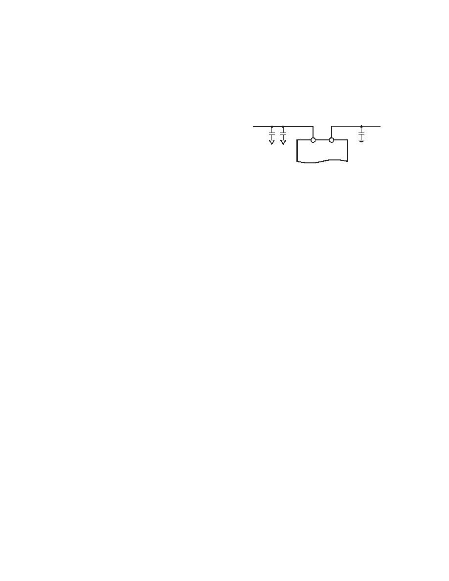
POWER SUPPLIES AND GROUNDING
The analog and digital supplies to the AD7713 are independent
and separately pinned out to minimize coupling between the
analog and digital sections of the device. The digital filter will
provide rejection of broadband noise on the power supplies,
except at integer multiples of the modulator sampling frequency.
The digital supply (DVDD) must not exceed the analog positive
supply (AVDD) by more than 0.3 V. If separate analog and digital
supplies are used, the recommended decoupling scheme is shown
in Figure 9. In systems where AVDD = 5 V and DVDD = 5 V, it is
recommended that AVDD and DVDD are driven from the same 5 V
supply, although each supply should be decoupled separately as
shown in Figure 9. It is preferable that the common supply is the
system’s analog 5 V supply.
It is also important that power is applied to the AD7713 before
signals at REF IN, AIN, or the logic input pins in order to avoid
excessive current. If separate supplies are used for the AD7713 and
the system digital circuitry, then the AD7713 should be powered
up first. If it is not possible to guarantee this, then current limiting
resistors should be placed in series with the logic inputs.
AD7713
0.1 F
10 F
ANALOG
SUPPLY
DIGITAL 5V
SUPPLY
AVDD
DVDD
Figure 9. Recommended Decoupling Scheme
DIGITAL INTERFACE
The AD7713’s serial communications port provides a flexible
arrangement to allow easy interfacing to industry-standard
microprocessors, microcontrollers, and digital signal processors.
A serial read to the AD7713 can access data from the output
register, the control register, or from the calibration registers. A
serial write to the AD7713 can write data to the control register
or the calibration registers.
Two different modes of operation are available, optimized for
different types of interface where the AD7713 can act either as
master in the system (it provides the serial clock) or as slave (an
external serial clock can be provided to the AD7713). These
two modes, labeled self-clocking mode and external clocking
mode, are discussed in detail in the following sections.
Self-Clocking Mode
The AD7713 is configured for its self-clocking mode by tying
the MODE pin high. In this mode, the AD7713 provides the
serial clock signal used for the transfer of data to and from the
AD7713. This self-clocking mode can be used with processors
that allow an external device to clock their serial port, including
most digital signal processors and microcontrollers, such as the
68HC11 and 68HC05. It also allows easy interfacing, to serial
parallel conversion circuits in systems with parallel data com-
munication, allowing interfacing to 74XX299 universal shift
registers without any additional decoding. In the case of shift
registers, the serial clock line should have a pull-down resistor
instead of the pull-up resistor shown in Figure 10 and Figure 11.
Read Operation
Data can be read from either the output register, the control
register, or the calibration registers. A0 determines whether the
data read accesses data from the control register or from the
output/calibration registers. This A0 signal must remain valid for
the duration of the serial read operation. With A0 high, data is
accessed from either the output register or from the calibration
registers. With A0 low, data is accessed from the control register.
The function of the
DRDY line is dependent on only the output
update rate of the device and the reading of the output data
register.
DRDY goes low when a new data-word is available in
the output data register. It is reset high when the last bit of data
(either 16th bit or 24th bit) is read from the output register. If
data is not read from the output register, the
DRDY line will
remain low. The output register will continue to be updated at
the output update rate, but
DRDY will not indicate this. A read
from the device in this circumstance will access the most recent
相关PDF资料 |
PDF描述 |
|---|---|
| MS27467T9B44S | CONN PLUG 4POS STRAIGHT W/SCKT |
| AD977CRZ | IC ADC 16BIT 100KSPS 20SOIC |
| VI-2NR-MX-F1 | CONVERTER MOD DC/DC 7.5V 75W |
| AD7892ANZ-1 | IC ADC 12BIT LP 500KSPS 24DIP |
| VI-2NP-MX-F4 | CONVERTER MOD DC/DC 13.8V 75W |
相关代理商/技术参数 |
参数描述 |
|---|---|
| AD7713SQ | 制造商:Analog Devices 功能描述: 制造商:Rochester Electronics LLC 功能描述: |
| AD7714 | 制造商:AD 制造商全称:Analog Devices 功能描述:3 V/5 V, CMOS, 500 uA Signal Conditioning ADC |
| AD7714ACHIPS-3 | 制造商:AD 制造商全称:Analog Devices 功能描述:3 V/5 V, CMOS, 500 uA Signal Conditioning ADC |
| AD7714ACHIPS-5 | 制造商:AD 制造商全称:Analog Devices 功能描述:3 V/5 V, CMOS, 500 uA Signal Conditioning ADC |
发布紧急采购,3分钟左右您将得到回复。