- 您现在的位置:买卖IC网 > PDF目录10118 > AD7713ARZ-REEL (Analog Devices Inc)IC ADC 24BIT SIGMA-DELTA 24SOIC PDF资料下载
参数资料
| 型号: | AD7713ARZ-REEL |
| 厂商: | Analog Devices Inc |
| 文件页数: | 4/28页 |
| 文件大小: | 0K |
| 描述: | IC ADC 24BIT SIGMA-DELTA 24SOIC |
| 标准包装: | 1,000 |
| 位数: | 24 |
| 采样率(每秒): | 205 |
| 数据接口: | 串行 |
| 转换器数目: | 1 |
| 功率耗散(最大): | 5.5mW |
| 电压电源: | 模拟和数字 |
| 工作温度: | -40°C ~ 85°C |
| 安装类型: | 表面贴装 |
| 封装/外壳: | 24-SOIC(0.295",7.50mm 宽) |
| 供应商设备封装: | 24-SOIC W |
| 包装: | 带卷 (TR) |
| 输入数目和类型: | 1 个单端,单极;1 个差分,单极;1 个差分,双极 |
第1页第2页第3页当前第4页第5页第6页第7页第8页第9页第10页第11页第12页第13页第14页第15页第16页第17页第18页第19页第20页第21页第22页第23页第24页第25页第26页第27页第28页
REV. D
–12–
AD7713
Figures 2a and 2b gives similar information to that outlined in
Table I. In this plot, the output rms noise is shown for the full
range of available cutoff frequencies rather than for some typical
cutoff frequencies as in Tables I and II. The numbers given in
these plots are typical values at 25
°C.
GAIN OF 1
GAIN OF 2
GAIN OF 4
GAIN OF 8
0.1
1.0
1000.0
100.0
10.0
10000.0
10
100
1k
10k
NOTCH FREQUENCY (Hz)
OUTPUT
NOISE
(
V)
Figure 2a. Plot of Output Noise vs. Gain and Notch
Frequency (Gains of 1 to 8)
GAIN OF 16
GAIN OF 32
GAIN OF 64
GAIN OF 128
0.1
1.0
100.0
10.0
1000.0
10
100
1k
10k
NOTCH FREQUENCY (Hz)
OUTPUT
NOISE
(
V)
Figure 2b. Plot of Output Noise vs. Gain and Notch
Frequency (Gains of 16 to 128)
CIRCUIT DESCRIPTION
The AD7713 is a -
ADC with on-chip digital filtering, intended
for the measurement of wide dynamic range, low frequency signals,
such as those in industrial control or process control applications. It
contains a
-
(or charge balancing) ADC, a calibration
microcontroller with on-chip static RAM, a clock oscillator, a
digital filter, and a bidirectional serial communications port.
The part contains three analog input channels, two program-
mable gain differential input channels, and one programmable
gain high-level single-ended input channel. The gain range on
both inputs is from 1 to 128. For the AIN1 and AIN2 inputs,
this means that the input can accept unipolar signals of between
0 mV to 20 mV and 0 V to 2.5 V or bipolar signals in the range
from
±20 mV to ±2.5 V when the reference input voltage equals
2.5 V. The input voltage range for the AIN3 input is 4
VREF/
GAIN and is 0 V to 10 V with the nominal reference of 2.5 V and
a ANALOG gain of 1. The input signal to the selected analog
input channel is continuously sampled at a rate determined by
the frequency of the master clock, MCLK IN, and the selected
gain (see Table III). A charge balancing ADC ( -
modulator)
converts the sampled signal into a digital pulse train whose duty
cycle contains the digital information. The programmable gain
function on the analog input is also incorporated in this -
modulator with the input sampling frequency being modified to
give the higher gains. A sinc
3 digital low-pass filter processes the
output of the
-
modulator and updates the output register at
a rate determined by the first notch frequency of this filter. The
output data can be read from the serial port randomly or peri-
odically at any rate up to the output register update rate. The
first notch of this digital filter (and therefore its –3 dB frequency)
can be programmed via an on-chip control register. The
programmable range for this first notch frequency is from
1.952 Hz to 205.59 Hz, giving a programmable range for the
–3 dB frequency of 0.52 Hz to 53.9 Hz.
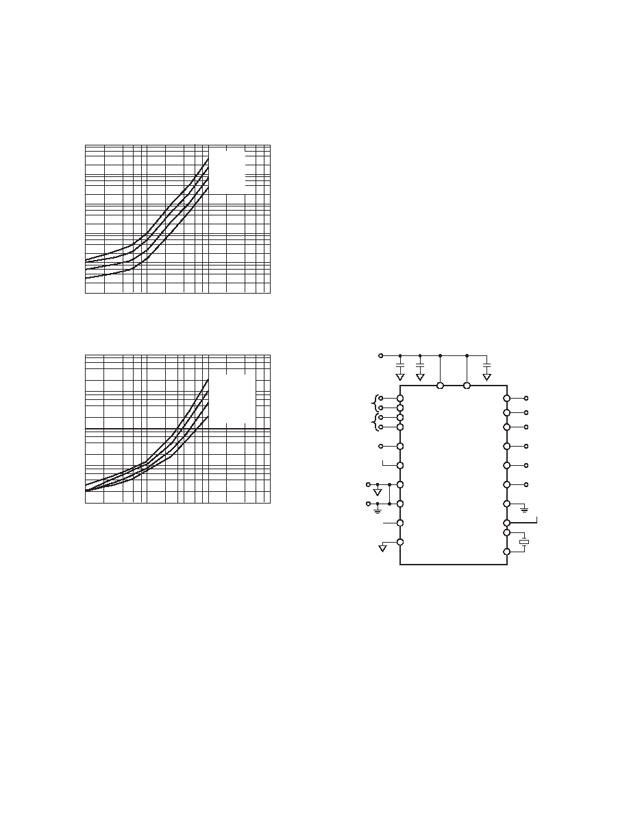
The basic connection diagram for the part is shown in Figure 3.
This shows the AD7713 in the external clocking mode with
both the AVDD and DVDD pins of the AD7713 being driven
from the analog 5 V supply. Some applications will have sepa-
rate supplies for both AVDD and DVDD, and in some of these
cases, the analog supply will exceed the 5 V digital supply (see the
Power Supplies and Grounding section).
REF IN(+)
AIN1(+)
AIN1(–)
AIN3
AVDD
DVDD
AGND
DGND
MCLK IN
MCLK OUT
REF IN(–)
ANALOG 5V
SUPPLY
0.1 F
10 F
AD7713
DIFFERENTIAL
ANALOG INPUT
SINGLE-ENDED
ANALOG INPUT
ANALOG
GROUND
DIGITAL
GROUND
MODE
DVDD
STANDBY
DVDD
AIN2(+)
AIN2(–)
2.5V
REFERENCE
DRDY
DATA
READY
TFS
TRANSMIT
(WRITE)
RFS
RECEIVE
(READ)
SDATA
SERIAL
DATA
SCLK
SERIAL
CLOCK
A0
ADDRESS
INPUT
DIFFERENTIAL
ANALOG INPUT
SYNC
Figure 3. Basic Connection Diagram
The AD7713 provides a number of calibration options that can
be programmed via the on-chip control register. A calibration
cycle can be initiated at any time by writing to this control regis-
ter. The part can perform self-calibration using the on-chip
calibration microcontroller and SRAM to store calibration
parameters. Other system components may also be included in
the calibration loop to remove offset and gain errors in the input
channel using the system calibration mode. Another option is a
background calibration mode where the part continuously
performs self-calibration and updates the calibration coeffi-
cients. Once the part is in this mode, the user does not have to
worry about issuing periodic calibration commands to the device
or asking the device to recalibrate when there is a change in the
ambient temperature or power supply voltage.
相关PDF资料 |
PDF描述 |
|---|---|
| MS27467T9B44S | CONN PLUG 4POS STRAIGHT W/SCKT |
| AD977CRZ | IC ADC 16BIT 100KSPS 20SOIC |
| VI-2NR-MX-F1 | CONVERTER MOD DC/DC 7.5V 75W |
| AD7892ANZ-1 | IC ADC 12BIT LP 500KSPS 24DIP |
| VI-2NP-MX-F4 | CONVERTER MOD DC/DC 13.8V 75W |
相关代理商/技术参数 |
参数描述 |
|---|---|
| AD7713SQ | 制造商:Analog Devices 功能描述: 制造商:Rochester Electronics LLC 功能描述: |
| AD7714 | 制造商:AD 制造商全称:Analog Devices 功能描述:3 V/5 V, CMOS, 500 uA Signal Conditioning ADC |
| AD7714ACHIPS-3 | 制造商:AD 制造商全称:Analog Devices 功能描述:3 V/5 V, CMOS, 500 uA Signal Conditioning ADC |
| AD7714ACHIPS-5 | 制造商:AD 制造商全称:Analog Devices 功能描述:3 V/5 V, CMOS, 500 uA Signal Conditioning ADC |
发布紧急采购,3分钟左右您将得到回复。