- 您现在的位置:买卖IC网 > PDF目录10667 > AD7719BRUZ (Analog Devices Inc)IC ADC 16BIT 24BIT DUAL 28-TSSOP PDF资料下载
参数资料
| 型号: | AD7719BRUZ |
| 厂商: | Analog Devices Inc |
| 文件页数: | 25/40页 |
| 文件大小: | 0K |
| 描述: | IC ADC 16BIT 24BIT DUAL 28-TSSOP |
| 标准包装: | 50 |
| 位数: | 16/24 |
| 采样率(每秒): | 105 |
| 数据接口: | DSP,MICROWIRE?,QSPI?,串行,SPI? |
| 转换器数目: | 2 |
| 功率耗散(最大): | 4.5mW |
| 电压电源: | 模拟和数字 |
| 工作温度: | -40°C ~ 85°C |
| 安装类型: | 表面贴装 |
| 封装/外壳: | 28-TSSOP(0.173",4.40mm 宽) |
| 供应商设备封装: | 28-TSSOP |
| 包装: | 管件 |
| 输入数目和类型: | 3 个差分,单极;3 个差分,双极 |
| 产品目录页面: | 778 (CN2011-ZH PDF) |
第1页第2页第3页第4页第5页第6页第7页第8页第9页第10页第11页第12页第13页第14页第15页第16页第17页第18页第19页第20页第21页第22页第23页第24页当前第25页第26页第27页第28页第29页第30页第31页第32页第33页第34页第35页第36页第37页第38页第39页第40页
REV. A
AD7719
–31–
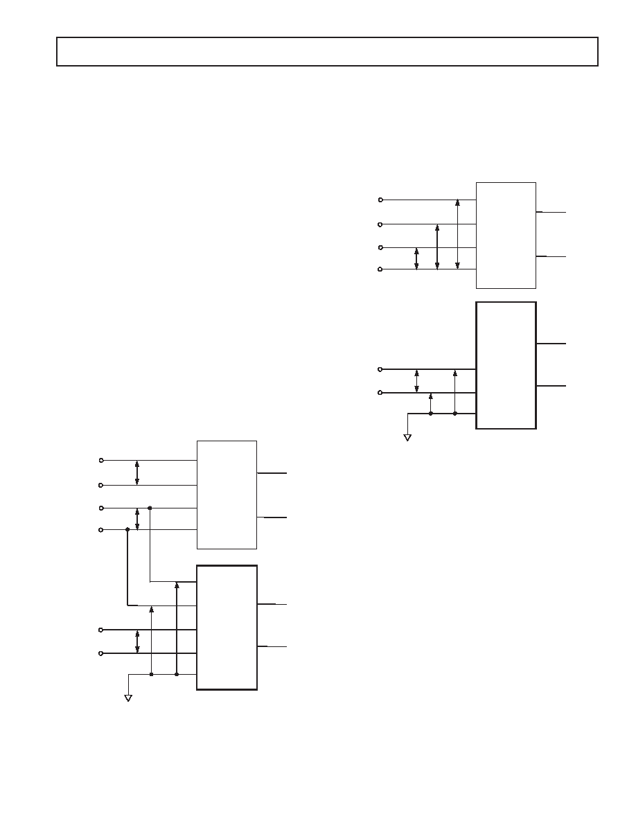
Analog Input Channels
The main ADC has four associated analog input pins (labeled
AIN1 to AIN4) that can be configured as two fully differential
input channels or three pseudodifferential input channels.
Channel selection bits CH1 and CH0 in the ADC0CON
register, along with the CHCON bit of the mode register,
detail the different configurations.
The auxiliary ADC has four external input pins (labeled AIN3
to AIN6) as well as an internal connection to the internal on-chip
temperature sensor. Channel selection bits ACH2, ACH1, and
ACH0 in the ADC1CON register, along with the CHCON
bit in the mode register, detail the various configurations on
these input channels.
Two input multiplexers (MUX1 and MUX2) switch the selected
input channel to the on-chip buffer amplifier in the case of the
main ADC when operated in buffered mode, and directly to the
Σ- modulator input in the case of the auxiliary ADC and when
the main ADC is operated in unbuffered mode. When the analog
input channel is switched, the settling time of the part must elapse
before a new valid word is available from the ADC.
Figure 16 shows the analog input channel configurations available
to the user when the CHCON bit in the mode register is set to a
zero. In this case, the main ADC can be configured as one or two
fully differential input channels (AIN1/AIN2 and AIN3/AIN4)
and the aux can be configured as two single-ended inputs with
respect to AGND (AIN3/AGND and AIN4/AGND) and one fully
differential input AIN5/AIN6). The aux can also be configured as
three single-ended inputs with respect to AGND (AIN3/AGND,
AIN4/AGND, and AIN5/AGND) by tying AIN6 externally to
AGND. The temp sensor is available as an internal connection.
SINGLE-
ENDED
INPUT
SINGLE-
ENDED
INPUT
FULLY DIFFERENTIAL
AIN(+)
AIN(–)
AIN(+)
AIN(–)
AIN1
AIN2
AIN3
AIN4
AIN1
AIN2
AIN3
AIN4
AIN5
AIN6
AIN3
AIN4
AGND
MUX1
(MAIN ADC)
(AUX ADC)
AIN5
AIN6
MAIN CHANNEL
AUX CHANNEL
MUX2
Figure 16. Input Channel Configurations with CHCON = 0
Figure 17 shows the analog input channel configurations avail-
able to the user when the CHCON bit in the mode register is
set to 1. In this case, the main ADC is configured as three
pseudodifferential input channels (AIN1/AIN4, AIN2/AIN4, and
AIN3/AIN4) and the aux can be configured as two single-ended
inputs with respect to AGND (AIN5/AGND and AIN6/AGND)
and one fully differential input (AIN5/AIN6). The temp sensor
is available as an internal connection.
SINGLE-
ENDED
INPUT
FULLY DIFFERENTIAL
AIN(+)
AIN(–)
AIN(+)
AIN(–)
AIN1
AIN2
AIN3
AIN4
AIN1
AIN2
AIN3
AIN4
AIN5
AIN6
AIN3
AIN4
AGND
MUX1
(MAIN ADC)
(AUX ADC)
AIN5
AIN6
SINGLE-
ENDED
INPUT
AIN3/AIN4
AIN2/AIN4
AIN1/AIN4
MUX2
MAIN CHANNEL
AUX CHANNEL
PSEUDO-
DIFFERENTIAL
INPUT
PSEUDO-
DIFFERENTIAL
INPUT
Figure 17. Input Channel Configurations with CHCON = 1
In buffered mode (
BUF = 0), the output of the main ADC multi-
plexer feeds into a high impedance input stage of the buffer
amplifier. As a result, the main ADC inputs can handle significant
source impedances and are tailored for direct connection to
external resistive-type sensors like strain gages or resistance
temperature detectors (RTDs).
The auxiliary ADC and the main ADC when operated with
BUF = 1, however, are unbuffered, resulting in higher analog
input current. It should be noted that these unbuffered input
paths provide a dynamic load to the driving source. Therefore,
resistor/capacitor combinations on the input pins can cause dc
gain errors, depending on the output impedance of the source
that is driving the ADC inputs. Table XVIII and XIX show the
allowable external resistance/capacitance values for unbuffered
mode such that no gain error at the 16- and 20-bit level,
respectively, is introduced.
The absolute input voltage range on the main ADC when oper-
ated in buffered mode is restricted to a range between AGND +
100 mV and AVDD – 100 mV. Care must be taken in setting up
the common-mode voltage and input voltage range so that these
limits are not exceeded; otherwise there will be a degradation in
linearity and noise performance.
相关PDF资料 |
PDF描述 |
|---|---|
| HA1-4902-2 | IC COMPARATOR QUAD PREC 16-DIP |
| LTC1417IGN#PBF | IC A/D CONV 14BIT SAMPLNG 16SSOP |
| AD7732BRUZ | IC ADC 24BIT 2-CH 28-TSSOP |
| LTC1418CG#PBF | IC A/D CONV 14BIT SRL&PAR 28SSOP |
| AD7574JNZ | IC ADC 8BIT CMOS 5V 18-DIP |
相关代理商/技术参数 |
参数描述 |
|---|---|
| AD7719BRUZ-REEL | 功能描述:IC ADC 16BIT 24BIT DUAL 28TSSOP RoHS:是 类别:集成电路 (IC) >> 数据采集 - 模数转换器 系列:- 标准包装:1,000 系列:- 位数:12 采样率(每秒):300k 数据接口:并联 转换器数目:1 功率耗散(最大):75mW 电压电源:单电源 工作温度:0°C ~ 70°C 安装类型:表面贴装 封装/外壳:24-SOIC(0.295",7.50mm 宽) 供应商设备封装:24-SOIC 包装:带卷 (TR) 输入数目和类型:1 个单端,单极;1 个单端,双极 |
| AD7719BRUZ-REEL7 | 功能描述:IC ADC 16BIT 24BIT DUAL 28TSSOP RoHS:是 类别:集成电路 (IC) >> 数据采集 - 模数转换器 系列:- 标准包装:1,000 系列:- 位数:12 采样率(每秒):300k 数据接口:并联 转换器数目:1 功率耗散(最大):75mW 电压电源:单电源 工作温度:0°C ~ 70°C 安装类型:表面贴装 封装/外壳:24-SOIC(0.295",7.50mm 宽) 供应商设备封装:24-SOIC 包装:带卷 (TR) 输入数目和类型:1 个单端,单极;1 个单端,双极 |
| AD7719BRZ | 功能描述:IC ADC 16BIT 24BIT DUAL 28SOIC RoHS:是 类别:集成电路 (IC) >> 数据采集 - 模数转换器 系列:- 标准包装:1,000 系列:- 位数:12 采样率(每秒):300k 数据接口:并联 转换器数目:1 功率耗散(最大):75mW 电压电源:单电源 工作温度:0°C ~ 70°C 安装类型:表面贴装 封装/外壳:24-SOIC(0.295",7.50mm 宽) 供应商设备封装:24-SOIC 包装:带卷 (TR) 输入数目和类型:1 个单端,单极;1 个单端,双极 |
| AD7720 | 制造商:AD 制造商全称:Analog Devices 功能描述:CMOS Sigma-Delta Modulator |
| AD7720BRU | 功能描述:IC MODULATOR SIGMA-DELTA 28TSSOP RoHS:否 类别:集成电路 (IC) >> 数据采集 - 模数转换器 系列:- 标准包装:1,000 系列:- 位数:12 采样率(每秒):300k 数据接口:并联 转换器数目:1 功率耗散(最大):75mW 电压电源:单电源 工作温度:0°C ~ 70°C 安装类型:表面贴装 封装/外壳:24-SOIC(0.295",7.50mm 宽) 供应商设备封装:24-SOIC 包装:带卷 (TR) 输入数目和类型:1 个单端,单极;1 个单端,双极 |
发布紧急采购,3分钟左右您将得到回复。