- 您现在的位置:买卖IC网 > PDF目录10667 > AD7719BRUZ (Analog Devices Inc)IC ADC 16BIT 24BIT DUAL 28-TSSOP PDF资料下载
参数资料
| 型号: | AD7719BRUZ |
| 厂商: | Analog Devices Inc |
| 文件页数: | 39/40页 |
| 文件大小: | 0K |
| 描述: | IC ADC 16BIT 24BIT DUAL 28-TSSOP |
| 标准包装: | 50 |
| 位数: | 16/24 |
| 采样率(每秒): | 105 |
| 数据接口: | DSP,MICROWIRE?,QSPI?,串行,SPI? |
| 转换器数目: | 2 |
| 功率耗散(最大): | 4.5mW |
| 电压电源: | 模拟和数字 |
| 工作温度: | -40°C ~ 85°C |
| 安装类型: | 表面贴装 |
| 封装/外壳: | 28-TSSOP(0.173",4.40mm 宽) |
| 供应商设备封装: | 28-TSSOP |
| 包装: | 管件 |
| 输入数目和类型: | 3 个差分,单极;3 个差分,双极 |
| 产品目录页面: | 778 (CN2011-ZH PDF) |
第1页第2页第3页第4页第5页第6页第7页第8页第9页第10页第11页第12页第13页第14页第15页第16页第17页第18页第19页第20页第21页第22页第23页第24页第25页第26页第27页第28页第29页第30页第31页第32页第33页第34页第35页第36页第37页第38页当前第39页第40页
REV. A
AD7719
–8–
DIGITAL INTERFACE
As previously outlined, the AD7719’s programmable functions are
controlled using a set of on-chip registers. Data is written to these
registers via the part’s serial interface; read access to the on-chip
registers is also provided by this interface. All communications to
the part must start with a write operation to the Communications
register. After power-on or
RESET, the device expects a write to
its Communications register. The data written to this register
determines whether the next operation to the part is a read or a
write operation and also determines to which register this read
or write operation occurs. Therefore, write access to any of the
other registers on the part starts with a write operation to the
Communications register followed by a write to the selected
register. A read operation from any other register on the part
(including the output data register) starts with a write operation
to the Communications register followed by a read operation
from the selected register.
The AD7719’s serial interface consists of five signals:
CS, SCLK,
DIN, DOUT, and
RDY. The DIN line is used for transferring
data into the on-chip registers while the DOUT line is used for
accessing data from the on-chip registers. SCLK is the serial
clock input for the device, and all data transfers (either on DIN
or DOUT) take place with respect to this SCLK signal. The
RDY line is used as a status signal to indicate when data is ready
to be read from the AD7719’s data register.
RDY goes low when a
new data-word is available in the output register of either the
main or aux ADCs. It is reset high when a read operation from
the data register is complete. It also goes high prior to the updating
of the output register to indicate when not to read from the device
to ensure that a data read is not attempted while the register is
being updated.
CS is used to select the device. It can be used to
decode the AD7719 in systems where a number of parts are
connected to the serial bus.
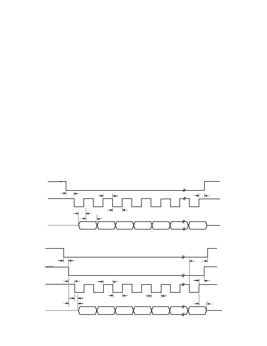
Figures 2 and 3 show timing diagrams for interfacing to the
AD7719 with
CS used to decode the part. Figure 3 is for a read
operation from the AD7719’s output shift register while Figure 2
shows a write operation to the input shift register. It is possible
to read the same data twice from the output register even though
the
RDY line returns high after the first read operation. Care must
be taken, however, to ensure that the read operations have been
completed before the next output update is about to take place.
The AD7719 serial interface can operate in 3-wire mode by tying
the
CS input low. In this case, the SCLK, DIN, and DOUT lines
are used to communicate with the AD7719, and the status of
RDY bits (RDY0 and RDY1) can be obtained by interrogating
the STATUS register. This scheme is suitable for interfacing to
microcontrollers. If
CS is required as a decoding signal, it can
be generated from a port bit. For microcontroller interfaces, it is
recommended that the SCLK idles high between data transfers.
The AD7719 can also be operated with
CS used as a frame syn-
chronization signal. This scheme is suitable for DSP interfaces.
In this case, the first bit (MSB) is effectively clocked out by
CS
since
CS would normally occur after the falling edge of SCLK
in DSPs. The SCLK can continue to run between data transfers
provided the timing numbers are obeyed.
t12
t13
t14
t15
t11
t16
MSB
LSB
CS
SCLK
DIN
Figure 2. Write Cycle Timing Diagram
t5
t5A
t4
t6
t3
t9
MSB
LSB
CS
SCLK
t8
t10
t7
t6
DOUT
RDY
Figure 3. Read Cycle Timing Diagram
相关PDF资料 |
PDF描述 |
|---|---|
| HA1-4902-2 | IC COMPARATOR QUAD PREC 16-DIP |
| LTC1417IGN#PBF | IC A/D CONV 14BIT SAMPLNG 16SSOP |
| AD7732BRUZ | IC ADC 24BIT 2-CH 28-TSSOP |
| LTC1418CG#PBF | IC A/D CONV 14BIT SRL&PAR 28SSOP |
| AD7574JNZ | IC ADC 8BIT CMOS 5V 18-DIP |
相关代理商/技术参数 |
参数描述 |
|---|---|
| AD7719BRUZ-REEL | 功能描述:IC ADC 16BIT 24BIT DUAL 28TSSOP RoHS:是 类别:集成电路 (IC) >> 数据采集 - 模数转换器 系列:- 标准包装:1,000 系列:- 位数:12 采样率(每秒):300k 数据接口:并联 转换器数目:1 功率耗散(最大):75mW 电压电源:单电源 工作温度:0°C ~ 70°C 安装类型:表面贴装 封装/外壳:24-SOIC(0.295",7.50mm 宽) 供应商设备封装:24-SOIC 包装:带卷 (TR) 输入数目和类型:1 个单端,单极;1 个单端,双极 |
| AD7719BRUZ-REEL7 | 功能描述:IC ADC 16BIT 24BIT DUAL 28TSSOP RoHS:是 类别:集成电路 (IC) >> 数据采集 - 模数转换器 系列:- 标准包装:1,000 系列:- 位数:12 采样率(每秒):300k 数据接口:并联 转换器数目:1 功率耗散(最大):75mW 电压电源:单电源 工作温度:0°C ~ 70°C 安装类型:表面贴装 封装/外壳:24-SOIC(0.295",7.50mm 宽) 供应商设备封装:24-SOIC 包装:带卷 (TR) 输入数目和类型:1 个单端,单极;1 个单端,双极 |
| AD7719BRZ | 功能描述:IC ADC 16BIT 24BIT DUAL 28SOIC RoHS:是 类别:集成电路 (IC) >> 数据采集 - 模数转换器 系列:- 标准包装:1,000 系列:- 位数:12 采样率(每秒):300k 数据接口:并联 转换器数目:1 功率耗散(最大):75mW 电压电源:单电源 工作温度:0°C ~ 70°C 安装类型:表面贴装 封装/外壳:24-SOIC(0.295",7.50mm 宽) 供应商设备封装:24-SOIC 包装:带卷 (TR) 输入数目和类型:1 个单端,单极;1 个单端,双极 |
| AD7720 | 制造商:AD 制造商全称:Analog Devices 功能描述:CMOS Sigma-Delta Modulator |
| AD7720BRU | 功能描述:IC MODULATOR SIGMA-DELTA 28TSSOP RoHS:否 类别:集成电路 (IC) >> 数据采集 - 模数转换器 系列:- 标准包装:1,000 系列:- 位数:12 采样率(每秒):300k 数据接口:并联 转换器数目:1 功率耗散(最大):75mW 电压电源:单电源 工作温度:0°C ~ 70°C 安装类型:表面贴装 封装/外壳:24-SOIC(0.295",7.50mm 宽) 供应商设备封装:24-SOIC 包装:带卷 (TR) 输入数目和类型:1 个单端,单极;1 个单端,双极 |
发布紧急采购,3分钟左右您将得到回复。