- 您现在的位置:买卖IC网 > PDF目录10667 > AD7719BRUZ (Analog Devices Inc)IC ADC 16BIT 24BIT DUAL 28-TSSOP PDF资料下载
参数资料
| 型号: | AD7719BRUZ |
| 厂商: | Analog Devices Inc |
| 文件页数: | 26/40页 |
| 文件大小: | 0K |
| 描述: | IC ADC 16BIT 24BIT DUAL 28-TSSOP |
| 标准包装: | 50 |
| 位数: | 16/24 |
| 采样率(每秒): | 105 |
| 数据接口: | DSP,MICROWIRE?,QSPI?,串行,SPI? |
| 转换器数目: | 2 |
| 功率耗散(最大): | 4.5mW |
| 电压电源: | 模拟和数字 |
| 工作温度: | -40°C ~ 85°C |
| 安装类型: | 表面贴装 |
| 封装/外壳: | 28-TSSOP(0.173",4.40mm 宽) |
| 供应商设备封装: | 28-TSSOP |
| 包装: | 管件 |
| 输入数目和类型: | 3 个差分,单极;3 个差分,双极 |
| 产品目录页面: | 778 (CN2011-ZH PDF) |
第1页第2页第3页第4页第5页第6页第7页第8页第9页第10页第11页第12页第13页第14页第15页第16页第17页第18页第19页第20页第21页第22页第23页第24页第25页当前第26页第27页第28页第29页第30页第31页第32页第33页第34页第35页第36页第37页第38页第39页第40页
REV. A
AD7719
–32–
The absolute input voltage range on the auxiliary ADC and the
main ADC in unbuffered mode includes the range between
AGND – 30 mV to AVDD + 30 mV as a result of being unbuf-
fered. The negative absolute input voltage limit does allow
the possibility of monitoring small true bipolar signals with
respect to AGND.
Programmable Gain Amplifier
The output from the buffer on the main ADC is applied to the
input of the on-chip programmable gain amplifier (PGA). The
PGA can be programmed through eight different unipolar and
bipolar ranges. The PGA gain range is programmed via the
range bits in the ADC0CON register. With an external 2.5 V
reference applied, the unipolar ranges are 0 mV to 20 mV, 0 mV
to 40 mV, 0 mV to 80 mV, 0 mV to 160 mV, 0 mV to 320 mV,
0 mV to 640 mV, 0 V to 1.28 V and 0 V to 2.56 V while bipolar
ranges are ±20 mV, ±40 mV, ±80 mV, ±160 mV, ±320 mV,
±640 mV, ±1.28 V, and ±2.56 V. These are the ranges that
should appear at the input to the on-chip PGA. The ADC range
matching specification of 2 V (typ) across all ranges means that
calibration need only be carried out on a single range and does
not have to be repeated when the PGA range is changed. This is
a significant advantage when compared with similar ADCs
available on the market.
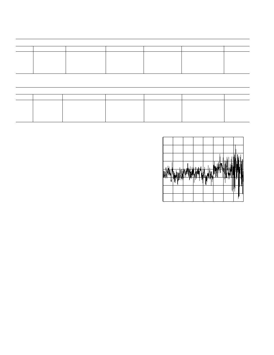
Typical matching across ranges is shown in Figure 18. Here, the
primary ADC is configured in fully differential, bipolar mode
with an external 2.5 V reference, while an analog input voltage
of just greater than 19 mV is forced on its analog inputs. The
ADC continuously converts the dc voltage at an update rate of
5.35 Hz, i.e., SF = 0xFF. In total, 800 conversion results are
gathered. The first 100 results are gathered with the primary ADC
operating in the ±20 mV range. The ADC range is then switched
to ±40 mV and 100 more results are gathered; this continues
until the last 100 samples are gathered with the ADC configured
in the ±2.5 V range. From Figure 18, the variation in the sample
mean through each range, i.e., the range matching, is seen to
be on the order of 2 V.
The auxiliary ADC does not incorporate an eight range PGA.
The aux ADC operates at a gain of 1 or a gain of 2 as determined
by the ARN bit in the AD1CON register.
0
100
200
300
400
500
600
700
800
SAMPLE COUNT
ADC
INPUT
VOLTAGE
(mV)
19.372
19.371
19.370
19.369
19.368
19.367
19.366
19.365
19.364
ADC RANGE
20mV
40mV
80mV
160mV
320mV
640mV
1.28V
2.56V
Figure 18. Main ADC Range Matching
Bipolar/Unipolar Configuration
The analog inputs on the AD7719 can accept either unipolar or
bipolar input voltage ranges. Bipolar input ranges do not imply that
the part can handle negative voltages with respect to system
AGND. Unipolar and bipolar signals on the AIN(+) input on
the main ADC are referenced to the voltage on the respective
AIN(–) input. AIN(+) and AIN(–) refer to the signals seen by
the modulator that come from the output of the multiplexer, as
shown in Figures 16 and 17.
For example, if AIN(–) is 2.5 V and the main ADC is config-
ured for an analog input range of 0 mV to 20 mV, the input
voltage range on the AIN(+) input is 2.5 V to 2.52 V. If AIN(–)
is 2.5 V and the AD7719 is configured for an analog input range
of ±1.28 V, the analog input range on the AIN(+) input is 1.22 V
to 3.78 V (i.e., 2.5 V ± 1.28 V). Bipolar or unipolar options are
chosen by programming the main and auxiliary U/
B bit in the
ADC0CON and ADC1CON registers, respectively. This pro-
grams the relevant ADC for either unipolar or bipolar operation.
Programming for either unipolar or bipolar operation does not
change any of the input signal conditioning; it simply changes the
data output coding and the points on the transfer function
where calibrations occur.
Table XVIII. Max Resistance for No 16-Bit Gain Error (Unbuffered Mode)
External Capacitance
Gain
0 pF
50 pF
100 pF
500 pF
1000 pF
5000 pF
1
111.3K
27.8K
16.7K
4.5K
2.58K
700
2
53.7K
13.5K
8.1K
2.2K
1.26K
360
4
25.4K
6.4K
3.9K
1.0K
600
170
8–128
10.7K
2.9K
1.7K
480
270
75
Table XIX. Max Resistance for No 20-Bit Gain Error (Unbuffered Mode)
External Capacitance
Gain
0 pF
50 pF
100 pF
500 pF
1000 pF
5000 pF
1
84.9K
21.1K
12.5K
3.2K
1.77K
440
2
42.0K
10.4K
6.1K
1.6K
880
220
4
20.5K
5.0K
2.9K
790K
430
110
8–128
8.8K
2.3K
1.3K
370
195
50
相关PDF资料 |
PDF描述 |
|---|---|
| HA1-4902-2 | IC COMPARATOR QUAD PREC 16-DIP |
| LTC1417IGN#PBF | IC A/D CONV 14BIT SAMPLNG 16SSOP |
| AD7732BRUZ | IC ADC 24BIT 2-CH 28-TSSOP |
| LTC1418CG#PBF | IC A/D CONV 14BIT SRL&PAR 28SSOP |
| AD7574JNZ | IC ADC 8BIT CMOS 5V 18-DIP |
相关代理商/技术参数 |
参数描述 |
|---|---|
| AD7719BRUZ-REEL | 功能描述:IC ADC 16BIT 24BIT DUAL 28TSSOP RoHS:是 类别:集成电路 (IC) >> 数据采集 - 模数转换器 系列:- 标准包装:1,000 系列:- 位数:12 采样率(每秒):300k 数据接口:并联 转换器数目:1 功率耗散(最大):75mW 电压电源:单电源 工作温度:0°C ~ 70°C 安装类型:表面贴装 封装/外壳:24-SOIC(0.295",7.50mm 宽) 供应商设备封装:24-SOIC 包装:带卷 (TR) 输入数目和类型:1 个单端,单极;1 个单端,双极 |
| AD7719BRUZ-REEL7 | 功能描述:IC ADC 16BIT 24BIT DUAL 28TSSOP RoHS:是 类别:集成电路 (IC) >> 数据采集 - 模数转换器 系列:- 标准包装:1,000 系列:- 位数:12 采样率(每秒):300k 数据接口:并联 转换器数目:1 功率耗散(最大):75mW 电压电源:单电源 工作温度:0°C ~ 70°C 安装类型:表面贴装 封装/外壳:24-SOIC(0.295",7.50mm 宽) 供应商设备封装:24-SOIC 包装:带卷 (TR) 输入数目和类型:1 个单端,单极;1 个单端,双极 |
| AD7719BRZ | 功能描述:IC ADC 16BIT 24BIT DUAL 28SOIC RoHS:是 类别:集成电路 (IC) >> 数据采集 - 模数转换器 系列:- 标准包装:1,000 系列:- 位数:12 采样率(每秒):300k 数据接口:并联 转换器数目:1 功率耗散(最大):75mW 电压电源:单电源 工作温度:0°C ~ 70°C 安装类型:表面贴装 封装/外壳:24-SOIC(0.295",7.50mm 宽) 供应商设备封装:24-SOIC 包装:带卷 (TR) 输入数目和类型:1 个单端,单极;1 个单端,双极 |
| AD7720 | 制造商:AD 制造商全称:Analog Devices 功能描述:CMOS Sigma-Delta Modulator |
| AD7720BRU | 功能描述:IC MODULATOR SIGMA-DELTA 28TSSOP RoHS:否 类别:集成电路 (IC) >> 数据采集 - 模数转换器 系列:- 标准包装:1,000 系列:- 位数:12 采样率(每秒):300k 数据接口:并联 转换器数目:1 功率耗散(最大):75mW 电压电源:单电源 工作温度:0°C ~ 70°C 安装类型:表面贴装 封装/外壳:24-SOIC(0.295",7.50mm 宽) 供应商设备封装:24-SOIC 包装:带卷 (TR) 输入数目和类型:1 个单端,单极;1 个单端,双极 |
发布紧急采购,3分钟左右您将得到回复。