- 您现在的位置:买卖IC网 > PDF目录10212 > AD7731BRZ-REEL (Analog Devices Inc)IC ADC 24BIT SIGMA-DELTA 24-SOIC PDF资料下载
参数资料
| 型号: | AD7731BRZ-REEL |
| 厂商: | Analog Devices Inc |
| 文件页数: | 25/44页 |
| 文件大小: | 0K |
| 描述: | IC ADC 24BIT SIGMA-DELTA 24-SOIC |
| 标准包装: | 1,000 |
| 位数: | 24 |
| 采样率(每秒): | 6.4k |
| 数据接口: | DSP,串行,SPI? |
| 转换器数目: | 1 |
| 功率耗散(最大): | 125mW |
| 电压电源: | 模拟和数字 |
| 工作温度: | -40°C ~ 85°C |
| 安装类型: | 表面贴装 |
| 封装/外壳: | 24-SOIC(0.295",7.50mm 宽) |
| 供应商设备封装: | 24-SOIC W |
| 包装: | 带卷 (TR) |
| 输入数目和类型: | 3 个差分,单极;3 个差分,双极;5 个伪差分,单极;5 个伪差分,双极 |
| 配用: | EVAL-AD7731EBZ-ND - BOARD EVALUATION FOR AD7731 |
第1页第2页第3页第4页第5页第6页第7页第8页第9页第10页第11页第12页第13页第14页第15页第16页第17页第18页第19页第20页第21页第22页第23页第24页当前第25页第26页第27页第28页第29页第30页第31页第32页第33页第34页第35页第36页第37页第38页第39页第40页第41页第42页第43页第44页
AD7731
–31–
REV. 0
The system full-scale calibration needs to be performed as one
part of a two part full calibration. However, once a full calibra-
tion has been performed, additional system full-scale calibra-
tions can be performed by themselves to adjust the part’s gain
calibration point only. When performing a two-step full calibra-
tion, care should be taken as to the sequence in which the two
steps are performed. A system full-scale calibration should not
be carried out unless the part contains valid zero-scale coeffi-
cients. Therefore, an internal zero-scale calibration or a system
zero-scale calibration must be performed before the system full-
scale calibration when a full two-step calibration operation is
being performed.
Span and Offset Limits
Whenever a system calibration mode is used, there are limits on
the amount of offset and span that can be accommodated. The
overriding requirement in determining the amount of offset and
gain that can be accommodated by the part is the requirement
that the positive full-scale calibration limit is
≤ 1.05 × FS, where
FS is 20 mV through 1.28 V depending on the RN2, RN1, RN0
bits in the Mode Register. This allows the input range to go 5%
above the nominal range. The built-in headroom in the AD7731’s
analog modulator ensures that the part will still operate correctly
with a positive full-scale voltage that is 5% beyond the nominal.
The range of input span in both the unipolar and bipolar modes
has a minimum value of 0.8
× FS and a maximum value of
2.1
× FS. However, the span (which is the difference between
the bottom of the AD7731’s input range and the top of its input
range) has to take into account the limitation on the positive
full-scale voltage. The amount of offset which can be accommo-
dated depends on whether the unipolar or bipolar mode is being
used. Once again, the offset has to take into account the limita-
tion on the positive full-scale voltage. In unipolar mode, there is
considerable flexibility in handling negative (with respect to
AIN[–]) offsets. In both unipolar and bipolar modes, the range
of positive offsets that can be handled by the part depends on
the selected span. Therefore, in determining the limits for sys-
tem zero-scale and full-scale calibrations, the user has to ensure
that the offset range plus the span range does not exceed
1.05
× FS. This is best illustrated by looking at a few examples.
If the part is used in unipolar mode with a required span of
0.8
× FS, the offset range the system calibration can handle is
from –1.05
× FS to +0.25 × FS. If the part is used in unipolar
mode with a required span of FS, the offset range the system
calibration can handle is from –1.05
× FS to +0.05 × FS. Simi-
larly, if the part is used in unipolar mode and required to remove
an offset of 0.2
× FS, the span range the system calibration can
handle is 0.85
× FS.
If the part is used in bipolar mode with a required span of
±0.4 × FS, the offset range the system calibration can handle is
from –0.65
× FS to +0.65 × FS. If the part is used in bipolar
mode with a required span of
±FS, the offset range the system
calibration can handle is from –0.05
× FS to +0.05 × FS. Simi-
larly, if the part is used in bipolar mode and required to remove
an offset of
±0.2 × FS, the span range the system calibration can
handle is
±0.85 × FS. Figure 14 summarizes the span and offset
ranges.
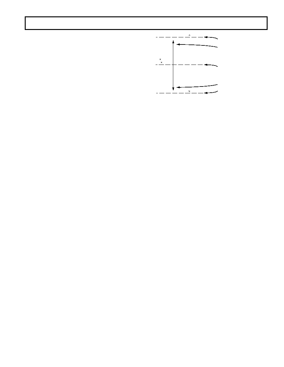
UPPER LIMIT. AD7731’s INPUT
VOLTAGE CANNOT EXCEED THIS
0V DIFFERENTIAL
1.05
FS.
NOMINAL ZERO-SCALE POINT
–1.05
FS.
LOWER LIMIT. AD7731’s INPUT
VOLTAGE CANNOT EXCEED THIS
AD7731
INPUT RANGE
(0.8
FS TO
2.1
FS)
GAIN CALIBRATIONS EXPAND OR
CONTRACT THE AD7731’s INPUT
RANGE
ZERO-SCALE CALIBRATIONS
MOVE INPUT RANGE UP OR DOWN
Figure 14. Span and Offset Limits
Power-Up and Calibration
On power-up, the AD7731 performs an internal reset that sets
the contents of the internal registers to a known state. There are
default values loaded to all registers after a power-on or reset.
The default values contain nominal calibration coefficients for
the calibration registers. However, to ensure correct calibration
for the device, a calibration routine should be performed after
power-up.
The power dissipation and temperature drift of the AD7731 are
low and no warm-up time is required before the initial calibra-
tion is performed. However, if an external reference is being
used, this reference must have stabilized before calibration is
initiated. Similarly, if the clock source for the part is generated
from a crystal or resonator across the MCLK pins, the start-up
time for the oscillator circuit should elapse before a calibration
is initiated on the part (see below).
Drift Considerations
The AD7731 uses chopper stabilization techniques to minimize
input offset drift. Charge injection in the analog multiplexer and
dc leakage currents at the analog input are the primary sources
of offset voltage drift in the part. The dc input leakage current is
essentially independent of the selected gain. Gain drift within
the converter depends primarily upon the temperature tracking
of the internal capacitors. It is not affected by leakage currents.
When operating the part in CHOP mode (CHP = 1), the signal
chain including the first-stage filter is chopped. This chopping
reduces the overall offset drift to 5 nV/
°C. When operating in
CHOP mode, it is recommended to calibrate the AD7731 only
after power-up or reset to achieve the optimum drift perfor-
mance from the part. Integral and differential linearity errors are
not significantly affected by temperature changes.
Care must also be taken with external drift effects in order to
achieve optimum drift performance. The user has to be espe-
cially careful to avoid, as much as possible, thermocouple effects
from junctions of different materials. Devices should not be
placed in sockets when evaluating temperature drift, there should
be no links in series with the analog inputs and care must be
taken as to how the input voltage is applied to the input pins.
The true offset drift of the AD7731 itself can be evaluated by
performing temperature drift testing of the part with the
AIN(–)/AIN(–) input channel arrangement (i.e., internal
shorted input, test mode).
REV. A
相关PDF资料 |
PDF描述 |
|---|---|
| SP3076EEN-L/TR | IC TXRX RS485/RS422 ESD 14NSOIC |
| AD7667ACPZRL | IC ADC 16BIT UNIPOLAR 48LFCSP |
| SP3075EEN-L/TR | IC TXRX RS485/RS422 ESD 8NSOIC |
| AD7667ASTZRL | IC ADC 16BIT UNIPOLAR 48LQFP |
| SP3074EEN-L/TR | IC TXRX RS485/RS422 ESD 8NSOIC |
相关代理商/技术参数 |
参数描述 |
|---|---|
| AD7731BRZ-REEL7 | 功能描述:IC ADC 24BIT SIGMA-DELTA 24-SOIC RoHS:是 类别:集成电路 (IC) >> 数据采集 - 模数转换器 系列:- 标准包装:1,000 系列:- 位数:12 采样率(每秒):300k 数据接口:并联 转换器数目:1 功率耗散(最大):75mW 电压电源:单电源 工作温度:0°C ~ 70°C 安装类型:表面贴装 封装/外壳:24-SOIC(0.295",7.50mm 宽) 供应商设备封装:24-SOIC 包装:带卷 (TR) 输入数目和类型:1 个单端,单极;1 个单端,双极 |
| AD7731EB | 制造商:AD 制造商全称:Analog Devices 功能描述:Low Noise High Throughput 24-Bit Sigma-Delta ADC(411.99 k) |
| AD7732 | 制造商:AD 制造商全称:Analog Devices 功能描述:2-Channel, +-10 V Input Range, High Throughput, 24-Bit SIGMA- ADC |
| AD7732BRU | 功能描述:IC ADC 24BIT 2-CH 28-TSSOP RoHS:否 类别:集成电路 (IC) >> 数据采集 - 模数转换器 系列:- 标准包装:1,000 系列:- 位数:12 采样率(每秒):300k 数据接口:并联 转换器数目:1 功率耗散(最大):75mW 电压电源:单电源 工作温度:0°C ~ 70°C 安装类型:表面贴装 封装/外壳:24-SOIC(0.295",7.50mm 宽) 供应商设备封装:24-SOIC 包装:带卷 (TR) 输入数目和类型:1 个单端,单极;1 个单端,双极 |
| AD7732BRU-REEL | 制造商:Analog Devices 功能描述:ADC Single Delta-Sigma 15.437ksps 24-bit Serial 28-Pin TSSOP T/R 制造商:Analog Devices 功能描述:ADC SGL DELTA-SIGMA 15.437KSPS 24BIT SERL 28TSSOP - Tape and Reel |
发布紧急采购,3分钟左右您将得到回复。