参数资料
| 型号: | AD7793BRU |
| 厂商: | Analog Devices Inc |
| 文件页数: | 2/33页 |
| 文件大小: | 0K |
| 描述: | IC ADC 24BIT 3CH LP 16-TSSOP |
| 设计资源: | Fully Isolated Input Module Based on AD7793 and ADuM5401(CN0066) Fully Isolated Input Module Based on AD7793, ADuM5401, and a High Performance In-Amp (CN0067) |
| 标准包装: | 1 |
| 位数: | 24 |
| 采样率(每秒): | 500 |
| 数据接口: | DSP,MICROWIRE?,QSPI?,串行,SPI? |
| 转换器数目: | 1 |
| 功率耗散(最大): | 2.5mW |
| 电压电源: | 模拟和数字 |
| 工作温度: | -40°C ~ 105°C |
| 安装类型: | 表面贴装 |
| 封装/外壳: | 16-TSSOP(0.173",4.40mm 宽) |
| 供应商设备封装: | 16-TSSOP |
| 包装: | 管件 |
| 输入数目和类型: | 3 个差分,单极;3 个差分,双极 |
| 配用: | EVAL-AD7793EBZ-ND - BOARD EVALUATION FOR AD7793 |
第1页当前第2页第3页第4页第5页第6页第7页第8页第9页第10页第11页第12页第13页第14页第15页第16页第17页第18页第19页第20页第21页第22页第23页第24页第25页第26页第27页第28页第29页第30页第31页第32页第33页
AD7792/AD7793
Rev. B | Page 9 of 32
PIN CONFIGURATION AND FUNCTION DESCRIPTIONS
04
85
5-
00
5
1
2
3
4
5
6
7
8
16
15
14
13
12
11
10
9
CLK
CS
IOUT1
AIN2(+)
AIN1(–)
AIN1(+)
SCLK
DOUT/RDY
DVDD
AVDD
REFIN(–)/AIN3(–)
AIN2(–)
REFIN(+)/AIN3(+)
IOUT2
GND
DIN
AD7792/
AD7793
TOP VIEW
(Not to Scale)
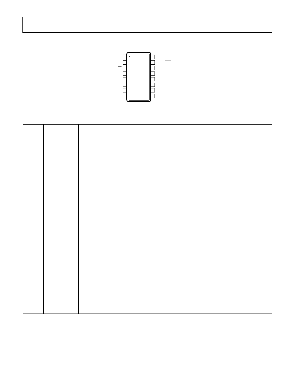
Figure 5. Pin Configuration
Table 4. Pin Function Descriptions
Pin No.
Mnemonic
Description
1
SCLK
Serial Clock Input. This serial clock input is for data transfers to and from the ADC. The SCLK has a Schmitt-
triggered input, making the interface suitable for opto-isolated applications. The serial clock can be
continuous with all data transmitted in a continuous train of pulses. Alternatively, it can be a noncontinuous
clock with the information being transmitted to or from the ADC in smaller batches of data.
2
CLK
Clock In/Clock Out. The internal clock can be made available at this pin. Alternatively, the internal clock can
be disabled, and the ADC can be driven by an external clock. This allows several ADCs to be driven from a
common clock, allowing simultaneous conversions to be performed.
3
CS
Chip Select Input. This is an active low logic input used to select the ADC. CS can be used to select the ADC
in systems with more than one device on the serial bus or as a frame synchronization signal in communicating
with the device. CS can be hardwired low, allowing the ADC to operate in 3-wire mode with SCLK, DIN, and
DOUT used to interface with the device.
4
IOUT1
Output of Internal Excitation Current Source. The internal excitation current source can be made available at
this pin. The excitation current source is programmable so that the current can be 10 μA, 210 μA, or 1 mA.
Either IEXC1 or IEXC2 can be switched to this output.
5
AIN1(+)
Analog Input. AIN1(+) is the positive terminal of the differential analog input pair AIN1(+)/AIN1(
).
6
AIN1(
)
Analog Input. AIN1(
) is the negative terminal of the differential analog input pair AIN1(+)/AIN1().
7
AIN2(+)
Analog Input. AIN2(+) is the positive terminal of the differential analog input pair AIN2(+)/AIN2(
).
8
AIN2(
)
Analog Input. AIN2(
) is the negative terminal of the differential analog input pair AIN2(+)/AIN2().
9
REFIN(+)/AIN3(+)
Positive Reference Input/Analog Input. An external reference can be applied between REFIN(+) and
REFIN(
). REFIN(+) can lie anywhere between AVDD and GND + 0.1 V. The nominal reference voltage
REFIN(+)
REFIN() is 2.5 V, but the part functions with a reference from 0.1 V to AVDD. Alternatively, this pin
can function as AIN3(+) where AIN3(+) is the positive terminal of the differential analog input pair
AIN3(+)/AIN3(
).
10
REFIN(
)/AIN3()
Negative Reference Input/Analog Input. REFIN(
) is the negative reference input for REFIN. This reference
input can lie anywhere between GND and AVDD
0.1 V. This pin also functions as AIN3(), which is the
negative terminal of the differential analog input pair AIN3(+)/AIN3(
).
11
IOUT2
Output of Internal Excitation Current Source. The internal excitation current source can be made available at
this pin. The excitation current source is programmable so that the current can be 10 μA, 210 μA, or 1 mA.
Either IEXC1 or IEXC2 can be switched to this output.
12
GND
Ground Reference Point.
13
AVDD
Supply Voltage, 2.7 V to 5.25 V.
14
DVDD
Digital Interface Supply Voltage. The logic levels for the serial interface pins are related to this supply, which
is between 2.7 V and 5.25 V. The DVDD voltage is independent of the voltage on AVDD; therefore, AVDD can
equal 5 V with DVDD at 3 V or vice versa.
相关PDF资料 |
PDF描述 |
|---|---|
| AD7794BRU | IC ADC 24BIT 6CH LP 24-TSSOP |
| AD7797BRUZ-REEL | IC ADC 24BIT SIG-DEL 1CH 16TSSOP |
| AD7799BRU | IC ADC 24BIT 3CH LP 16-TSSOP |
| AD7801BRU | IC DAC 8BIT PARALLEL INP 20TSSOP |
| AD7810YR | IC ADC 10BIT 2.7V 8-SOIC |
相关代理商/技术参数 |
参数描述 |
|---|---|
| AD7793BRU-REEL | 制造商:Analog Devices 功能描述:ADC Single Delta-Sigma 470sps 24-bit Serial 16-Pin TSSOP T/R 制造商:Analog Devices 功能描述:ADC SGL DELTA-SIGMA 0.47KSPS 24BIT SERL 16TSSOP - Tape and Reel |
| AD7793BRUZ | 功能描述:IC ADC 24BIT SIG-DEL 3CH 16TSSOP RoHS:是 类别:集成电路 (IC) >> 数据采集 - 模数转换器 系列:- 标准包装:1 系列:microPOWER™ 位数:8 采样率(每秒):1M 数据接口:串行,SPI? 转换器数目:1 功率耗散(最大):- 电压电源:模拟和数字 工作温度:-40°C ~ 125°C 安装类型:表面贴装 封装/外壳:24-VFQFN 裸露焊盘 供应商设备封装:24-VQFN 裸露焊盘(4x4) 包装:Digi-Reel® 输入数目和类型:8 个单端,单极 产品目录页面:892 (CN2011-ZH PDF) 其它名称:296-25851-6 |
| AD7793BRUZ1 | 制造商:AD 制造商全称:Analog Devices 功能描述:3-Channel, Low Noise, Low Power, 16-/24-Bit ?£-?? ADC with On-Chip In-Amp and Reference |
| AD7793BRUZ-REEL | 功能描述:IC ADC 24BIT 3CH LP 16-TSSOP RoHS:是 类别:集成电路 (IC) >> 数据采集 - 模数转换器 系列:- 标准包装:1,000 系列:- 位数:16 采样率(每秒):45k 数据接口:串行 转换器数目:2 功率耗散(最大):315mW 电压电源:模拟和数字 工作温度:0°C ~ 70°C 安装类型:表面贴装 封装/外壳:28-SOIC(0.295",7.50mm 宽) 供应商设备封装:28-SOIC W 包装:带卷 (TR) 输入数目和类型:2 个单端,单极 |
| AD7793BRUZ-REEL1 | 制造商:AD 制造商全称:Analog Devices 功能描述:3-Channel, Low Noise, Low Power, 16-/24-Bit ?£-?? ADC with On-Chip In-Amp and Reference |
发布紧急采购,3分钟左右您将得到回复。