参数资料
| 型号: | AD7891YPZ-1 |
| 厂商: | Analog Devices Inc |
| 文件页数: | 18/20页 |
| 文件大小: | 0K |
| 描述: | IC DAS 12BIT 8CH 44-PLCC |
| 标准包装: | 1 |
| 类型: | 数据采集系统(DAS) |
| 分辨率(位): | 12 b |
| 采样率(每秒): | 500k |
| 数据接口: | 串行,并联 |
| 电压电源: | 单电源 |
| 电源电压: | 5V |
| 工作温度: | -55°C ~ 105°C |
| 安装类型: | 表面贴装 |
| 封装/外壳: | 44-LCC(J 形引线) |
| 供应商设备封装: | 44-PLCC(16.59x16.59) |
| 包装: | 管件 |
AD7891
–7–
REV. D
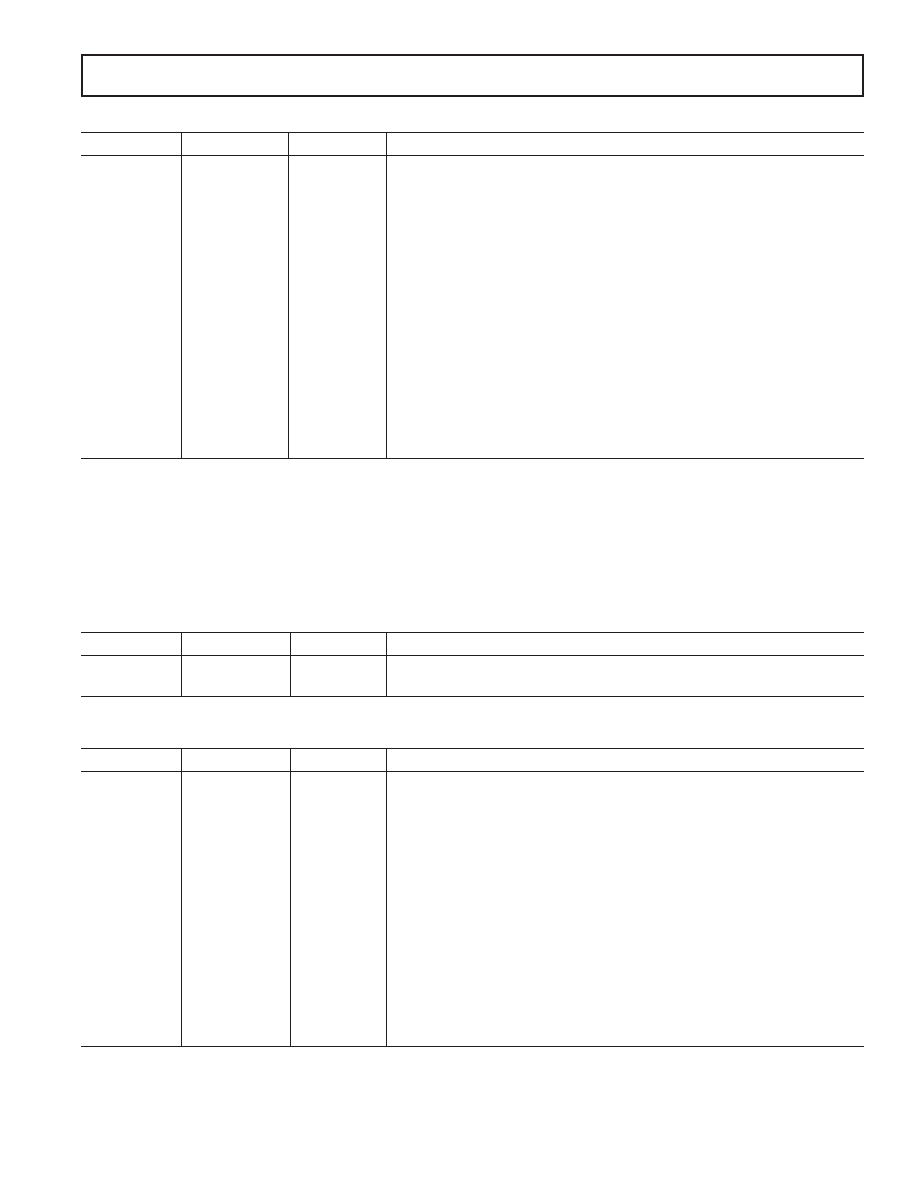
PARALLEL INTERFACE MODE FUNCTIONS
PLCC Pin No.
MQFP Pin No. Mnemonic
Description
8, 31
2, 25
NC
No Connect. The two NC pins on the device can be left unconnected. If they
are to be connected to a voltage, it should be to ground potential. To ensure
correct operation of the AD7891, neither of the NC pins should be connected
to a logic high potential.
29
23
CS
Chip Select Input. Active low logic input that is used in conjunction with to
enable the data outputs and with
WR to allow input data to be written to the part.
28
22
RD
Read Input. Active low logic input that is used in conjunction with
CS low to
enable the data outputs.
27
21
WR
Write Input. Active low logic input used in conjunction with
CS to latch the mul-
tiplexer address and software control information. The rising edge of this input
also initiates an internal pulse. When using the software start facility, this pulse
delays the point at which the track/hold goes into hold and conversion is initiated.
This allows the multiplexer to settle and the acquisition time of the track/hold to
elapse when a channel address is changed. If the SWCON bit of the control regis-
ter is set to 1, when this pulse times out, the track/hold then goes into hold and
conversion is initiated. If the SWCON bit of the control register is set to 0, the
track/hold and conversion sequence are unaffected by
WR operation.
Data I/O Lines
There are 12 data input/output lines on the AD7891. When the part is configured for parallel mode (MODE = 1), the output data
from the part is provided at these 12 pins during a read operation. For a write operation in parallel mode, these lines provide access
to the part’s control register.
Parallel Read Operation
During a parallel read operation, the 12 lines become the 12 data bits containing the conversion result from the AD7891. These
data bits are labelled Data Bit 0 (LSB) to Data Bit 11 (MSB). They are three-state, TTL compatible outputs. Output data coding
is twos complement when the data FORMAT bit of the control register is 1, and straight binary when the data FORMAT bit of
the control register is 0.
PLCC Pin No.
MQFP Pin No. Mnemonic
Description
13 to 18,
7 to 12,
DB0 to DB11 Data Bit 0 (LSB) to Data Bit 11 (MSB). Three-state TTL compatible
21 to 26
15 to 20
outputs that are controlled by the
CS and RD inputs.
Parallel Write Operation
During a parallel write operation, the following functions can be written to the control register via the 12 data input/output pins.
PLCC Pin No.
MQFP Pin No. Mnemonic
Description
23
17
A0
Address Input. The status of this input during a parallel write operation is
latched to the A0 bit of the control register (see Control Register section).
22
16
A1
Address Input. The status of this input during a parallel write operation is
latched to the A1 bit of the control register (see Control Register section).
21
15
A2
Address Input. The status of this input during a parallel write operation is
latched to the A2 bit of the control register (see Control Register section).
24
18
SWCON
Software Conversion Start. The status of this input during a parallel write
operation is latched to the SWCONV bit of the control register (see Control
Register section).
25
19
SWSTBY
Software Standby Control. The status of this input during a parallel write
operation is latched to the SWSTBY bit of the control register (see Control
Register section).
26
20
FORMAT
Data Format Selection. The status of this input during a parallel write operation is
latched to the FORMAT bit of the control register (see Control Register section).
相关PDF资料 |
PDF描述 |
|---|---|
| LTC6906IS6#TRMPBF | IC OSC SILICON 1MHZ TSOT23-6 |
| AD7891YSZ-2 | IC DAS 12BIT 8CH 44-MQFP |
| LTC6907IS6#TRPBF | IC OSC SILICON 4MHZ TSOT23-6 |
| LTC6906IS6#TRPBF | IC OSC SILICON 1MHZ TSOT23-6 |
| AD974AN | IC DAS 16BIT 4CH 200KSPS 28-DIP |
相关代理商/技术参数 |
参数描述 |
|---|---|
| AD7891YPZ-1REEL | 功能描述:IC DAS 12BIT 8CH 44-PLCC RoHS:是 类别:集成电路 (IC) >> 数据采集 - ADCs/DAC - 专用型 系列:- 产品培训模块:Lead (SnPb) Finish for COTS Obsolescence Mitigation Program 标准包装:50 系列:- 类型:数据采集系统(DAS) 分辨率(位):16 b 采样率(每秒):21.94k 数据接口:MICROWIRE?,QSPI?,串行,SPI? 电压电源:模拟和数字 电源电压:1.8 V ~ 3.6 V 工作温度:-40°C ~ 85°C 安装类型:表面贴装 封装/外壳:40-WFQFN 裸露焊盘 供应商设备封装:40-TQFN-EP(6x6) 包装:托盘 |
| AD7891YS1 | 制造商:AD 功能描述:New |
| AD7891YS-1 | 制造商:Analog Devices 功能描述:ADC Single 454.5ksps 12-bit Parallel/Serial 44-Pin MQFP |
| AD7891YS-1REEL | 制造商:Analog Devices 功能描述:ADC Single 454.5ksps 12-bit Parallel/Serial 44-Pin MQFP T/R 制造商:Analog Devices 功能描述:ADC SGL 454.5KSPS 12-BIT PARALLEL/SERL 44MQFP - Tape and Reel |
| AD7891YS-2 | 制造商:Analog Devices 功能描述:ADC Single 500ksps 12-bit Parallel/Serial 44-Pin MQFP 制造商:Rochester Electronics LLC 功能描述:8 CHANNEL, 12-BIT ADC I.C. - Bulk |
发布紧急采购,3分钟左右您将得到回复。