参数资料
| 型号: | AD7891YPZ-1 |
| 厂商: | Analog Devices Inc |
| 文件页数: | 7/20页 |
| 文件大小: | 0K |
| 描述: | IC DAS 12BIT 8CH 44-PLCC |
| 标准包装: | 1 |
| 类型: | 数据采集系统(DAS) |
| 分辨率(位): | 12 b |
| 采样率(每秒): | 500k |
| 数据接口: | 串行,并联 |
| 电压电源: | 单电源 |
| 电源电压: | 5V |
| 工作温度: | -55°C ~ 105°C |
| 安装类型: | 表面贴装 |
| 封装/外壳: | 44-LCC(J 形引线) |
| 供应商设备封装: | 44-PLCC(16.59x16.59) |
| 包装: | 管件 |
AD7891
–15–
REV. D
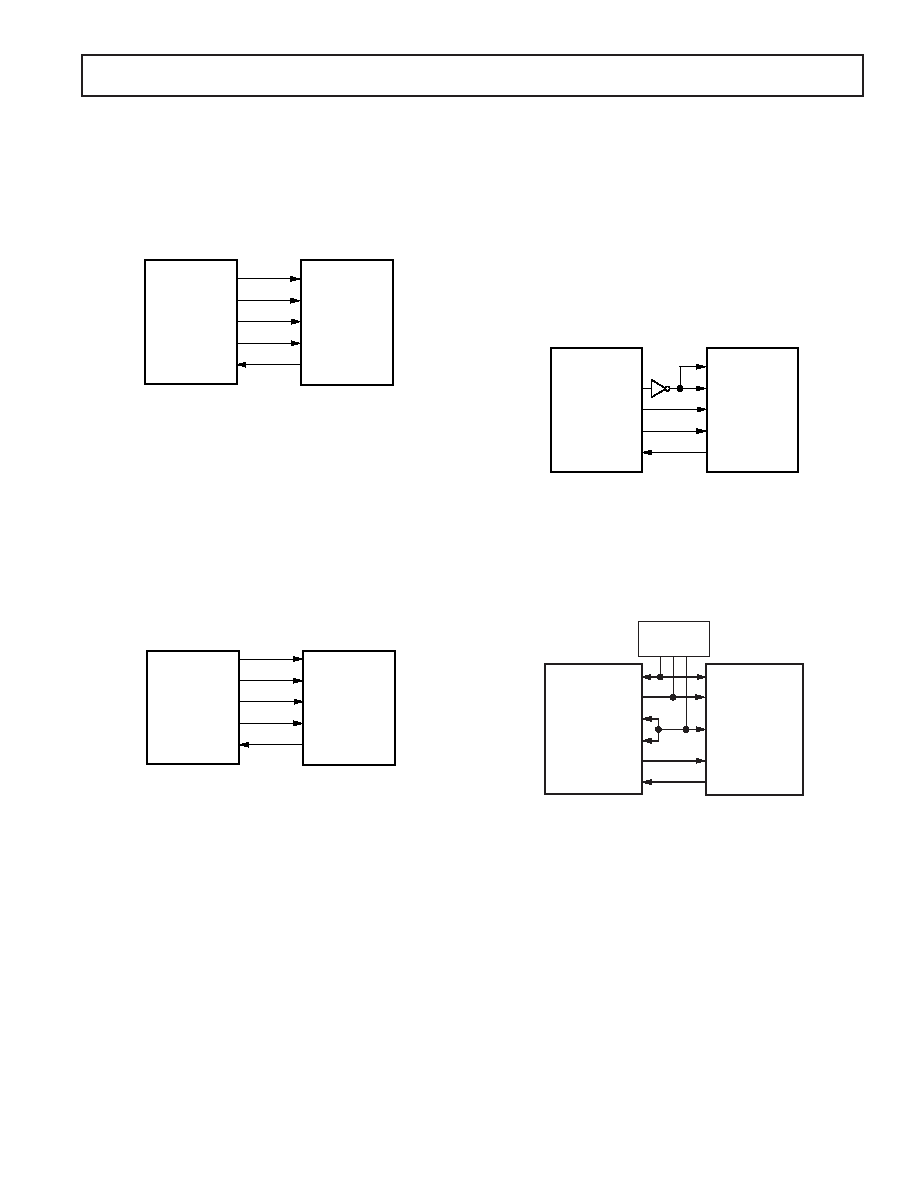
As in the 8X51 circuit in Figure 7, the way the 68HC11 is
informed that a conversion is completed is not shown in the
diagram. The
EOC line can be used to inform the 68HC11
that a conversion is complete by using it as an interrupt signal.
The interrupt service routine reads in the result of the conver-
sion. If a software conversion start is used, the 68HC11 can
wait for 2.0
ms (AD7891-2) or 2.2 ms (AD7891-1) before read-
ing from the AD7891.
68HC11*
DATA OUT
AD7891*
*ADDITIONAL PINS OMITTED FOR CLARITY
SCLK
DATA IN
RFS
TFS
PC7
PC6
SCK
MOSI
MOSO
Figure 8. AD7891 to 68HC11 Interface
AD7891 to ADSP-21xx Serial Interface
An interface between the AD7891 and the ADSP-21xx is shown
in Figure 9. In the interface shown, either SPORT0 or SPORT1
can be used to transfer data to the AD7891. When reading
from the part, the SPORT must be set up with a serial word
length of 16 bits. When writing to the AD7891, a serial word
length of 6 bits or more can be used. Other setups for the
serial interface on the ADSP-21xx internal SCLK use alternate
framing mode and active low framing signal. Normally, the
EOC line from the AD7891 would be connected to the IRQ2
line of the ADSP-21xx to interrupt the DSP at the end of a
conversion (not shown in diagram).
ADSP-21xx*
DATA OUT
AD7891*
*ADDITIONAL PINS OMITTED FOR CLARITY
SCLK
DATA IN
RFS
TFS
RFS
TFS
SCLK
DT
DR
Figure 9. AD7891 to ADSP-21xx Serial Interface
AD7891 to DSP5600x Serial Interface
Figure 10 shows a serial interface between the AD7891 and the
DSP5600x series of DSPs. When reading from the AD7891, the
DSP5600x should be set up for 16-bit data transfers, MSB first,
normal mode synchronous operation, internally generated word
frame sync, and gated clock. When writing to the AD7891, 8-bit
or 16-bit data transfers can be used. The frame sync signal from
the DSP5600x must be inverted before being applied to the
RFS and TFS inputs of the AD7891, as shown in Figure 10.
To monitor the conversion time of the AD7891, a scheme such
as those outlined in previous interfaces with
EOC can be used.
This can be implemented by connecting the
EOC line directly
to the
IRQA input of the DSP5600x.
DSP5600x*
DATA OUT
AD7891*
*ADDITIONAL PINS OMITTED FOR CLARITY
SCLK
DATA IN
RFS
TFS
FST (SC2)
SCK
STD
SRD
Figure 10. AD7891 to DSP5600x Serial Interface
AD7891 to TMS320xxx Serial Interface
The AD7891 can be interfaced to the serial port of TMS320xxx
DSPs, as shown in Figure 11. External timing generation circuitry
is necessary to generate the serial clock and syncs necessary for
the interface.
TMS320xxx*
DATA OUT
AD7891*
*ADDITIONAL PINS OMITTED FOR CLARITY
SCLK
DATA IN
RFS
TFS
FSX
CLKX
DX
DR
CLKR
FSR
TIMING
GENERATION
CIRCUITRY
Figure 11. AD7891 to TMS320xxx Serial Interface
相关PDF资料 |
PDF描述 |
|---|---|
| LTC6906IS6#TRMPBF | IC OSC SILICON 1MHZ TSOT23-6 |
| AD7891YSZ-2 | IC DAS 12BIT 8CH 44-MQFP |
| LTC6907IS6#TRPBF | IC OSC SILICON 4MHZ TSOT23-6 |
| LTC6906IS6#TRPBF | IC OSC SILICON 1MHZ TSOT23-6 |
| AD974AN | IC DAS 16BIT 4CH 200KSPS 28-DIP |
相关代理商/技术参数 |
参数描述 |
|---|---|
| AD7891YPZ-1REEL | 功能描述:IC DAS 12BIT 8CH 44-PLCC RoHS:是 类别:集成电路 (IC) >> 数据采集 - ADCs/DAC - 专用型 系列:- 产品培训模块:Lead (SnPb) Finish for COTS Obsolescence Mitigation Program 标准包装:50 系列:- 类型:数据采集系统(DAS) 分辨率(位):16 b 采样率(每秒):21.94k 数据接口:MICROWIRE?,QSPI?,串行,SPI? 电压电源:模拟和数字 电源电压:1.8 V ~ 3.6 V 工作温度:-40°C ~ 85°C 安装类型:表面贴装 封装/外壳:40-WFQFN 裸露焊盘 供应商设备封装:40-TQFN-EP(6x6) 包装:托盘 |
| AD7891YS1 | 制造商:AD 功能描述:New |
| AD7891YS-1 | 制造商:Analog Devices 功能描述:ADC Single 454.5ksps 12-bit Parallel/Serial 44-Pin MQFP |
| AD7891YS-1REEL | 制造商:Analog Devices 功能描述:ADC Single 454.5ksps 12-bit Parallel/Serial 44-Pin MQFP T/R 制造商:Analog Devices 功能描述:ADC SGL 454.5KSPS 12-BIT PARALLEL/SERL 44MQFP - Tape and Reel |
| AD7891YS-2 | 制造商:Analog Devices 功能描述:ADC Single 500ksps 12-bit Parallel/Serial 44-Pin MQFP 制造商:Rochester Electronics LLC 功能描述:8 CHANNEL, 12-BIT ADC I.C. - Bulk |
发布紧急采购,3分钟左右您将得到回复。