参数资料
| 型号: | AD7891YPZ-1 |
| 厂商: | Analog Devices Inc |
| 文件页数: | 2/20页 |
| 文件大小: | 0K |
| 描述: | IC DAS 12BIT 8CH 44-PLCC |
| 标准包装: | 1 |
| 类型: | 数据采集系统(DAS) |
| 分辨率(位): | 12 b |
| 采样率(每秒): | 500k |
| 数据接口: | 串行,并联 |
| 电压电源: | 单电源 |
| 电源电压: | 5V |
| 工作温度: | -55°C ~ 105°C |
| 安装类型: | 表面贴装 |
| 封装/外壳: | 44-LCC(J 形引线) |
| 供应商设备封装: | 44-PLCC(16.59x16.59) |
| 包装: | 管件 |
AD7891
–10–
REV. D
INTERFACE INFORMATION
The AD7891 provides two interface options, a 12-bit parallel
interface and a high speed serial interface. The required inter-
face mode is selected via the MODE pin. The two interface
modes are discussed in the following sections.
Parallel Interface Mode
The parallel interface mode is selected by tying the MODE
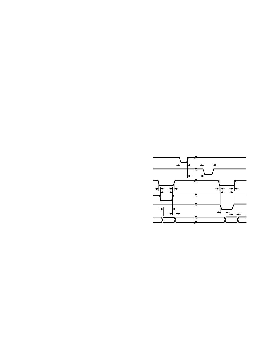
input to a logic high. Figure 2 shows a timing diagram illustrating
the operational sequence of the AD7891 in parallel mode for a
hardware conversion start. The multiplexer address is written to
the AD7891 on the rising edge of the
WR input. The on-chip
track/hold goes into hold mode on the rising edge of
CONVST;
conversion is also initiated at this point. When the conversion is
complete, the end of conversion line (
EOC) pulses low to indi-
cate that new data is available in the AD7891’s output register.
This
EOC line can be used to drive an edge-triggered interrupt
of a microprocessor.
CS and RD going low accesses the 12-bit
conversion result. In systems where the part is interfaced to a
gate array or ASIC, this
EOC pulse can be applied to the CS
and
RD inputs to latch data out of the AD7891 and into the
gate array or ASIC. This means the gate array or ASIC does not
need any conversion status recognition logic, and it also elimi-
nates the logic required in the gate array or ASIC to generate
the read signal for the AD7891.
t6
t7
tCONV
t1
t5
t8
t1
t5
t2
VALID DATA
OUTPUT
VALID DATA
INPUT
t9
t10
t3
t4
CONVST (I)
EOC (O)
CS (O)
WR (I)
RD (I)
DB0 TO DB11
(I/O)
NOTE
I = INPUT
O = OUTPUT
Figure 2. Parallel Mode Timing Diagram
CONVERTER DETAILS
The AD7891 is an 8-channel, high speed, 12-bit data acquisi-
tion system. It provides the user with signal scaling, multiplexer,
track/hold, reference, ADC, and high speed parallel and serial
interface logic functions on a single chip. The signal condition-
ing on the AD7891-1 allows the part to accept analog input
ranges of
±5V or ±10 V when operating from a single supply.
The input circuitry on the AD7891-2 allows the part to handle
input signal ranges of 0 V to +2.5 V, 0 V to +5 V, and
±2.5 V
again while operating from a single 5 V supply. The part requires
a 2.5 V reference that can be provided from the part’s own internal
reference or from an external reference source.
Conversion is initiated on the AD7891 either by pulsing the
CONVST input or by writing a Logic 1 to the SWCONV bit of
the control register. When using the hardware
CONVST input,
the on-chip track/hold goes from track to hold mode and the
conversion sequence is started on the rising edge of the
CONVST
signal. When a software conversion start is initiated, an internal
pulse is generated, delaying the track/hold acquisition point and
the conversion start sequence until the pulse is timed out. This
internal pulse is initiated (goes from low to high) whenever a
write to the AD7891 control register takes place with a 1 in the
SWCONV bit. It then starts to discharge and the track/hold
cannot go into hold and conversion cannot be initiated until the
pulse signal goes low. The internal pulse duration is equal to the
track/hold acquisition time. This allows the user to obtain a
valid result after changing channels and initiating a conversion
in the same write operation.
The conversion clock for the part is internally generated and
conversion time for the AD7891 is 1.6
ms from the rising edge of
the hardware
CONVST signal. The track/hold acquisition time
for the AD7891-1 is 600 ns, while the track/hold acquisition
time for the AD7891-2 is 400 ns. To obtain optimum perfor-
mance from the part, the data read operation should not occur
during the conversion or during the 100 ns prior to the next
conversion. This allows the AD7891-1 to operate at throughput
rates up to 454.5 kSPS and the AD7891-2 to operate at through-
put rates up to 500 kSPS in the parallel mode and achieve data
sheet specifications. In the serial mode, the maximum achievable
throughput rate for both the AD7891-1 and the AD7891-2 is
357 kSPS (assuming a 20 MHz serial clock).
All unused analog inputs should be tied to a voltage within the
nominal analog input range to avoid noise pickup. For mini-
mum power consumption, the unused analog inputs should be
tied to AGND.
相关PDF资料 |
PDF描述 |
|---|---|
| LTC6906IS6#TRMPBF | IC OSC SILICON 1MHZ TSOT23-6 |
| AD7891YSZ-2 | IC DAS 12BIT 8CH 44-MQFP |
| LTC6907IS6#TRPBF | IC OSC SILICON 4MHZ TSOT23-6 |
| LTC6906IS6#TRPBF | IC OSC SILICON 1MHZ TSOT23-6 |
| AD974AN | IC DAS 16BIT 4CH 200KSPS 28-DIP |
相关代理商/技术参数 |
参数描述 |
|---|---|
| AD7891YPZ-1REEL | 功能描述:IC DAS 12BIT 8CH 44-PLCC RoHS:是 类别:集成电路 (IC) >> 数据采集 - ADCs/DAC - 专用型 系列:- 产品培训模块:Lead (SnPb) Finish for COTS Obsolescence Mitigation Program 标准包装:50 系列:- 类型:数据采集系统(DAS) 分辨率(位):16 b 采样率(每秒):21.94k 数据接口:MICROWIRE?,QSPI?,串行,SPI? 电压电源:模拟和数字 电源电压:1.8 V ~ 3.6 V 工作温度:-40°C ~ 85°C 安装类型:表面贴装 封装/外壳:40-WFQFN 裸露焊盘 供应商设备封装:40-TQFN-EP(6x6) 包装:托盘 |
| AD7891YS1 | 制造商:AD 功能描述:New |
| AD7891YS-1 | 制造商:Analog Devices 功能描述:ADC Single 454.5ksps 12-bit Parallel/Serial 44-Pin MQFP |
| AD7891YS-1REEL | 制造商:Analog Devices 功能描述:ADC Single 454.5ksps 12-bit Parallel/Serial 44-Pin MQFP T/R 制造商:Analog Devices 功能描述:ADC SGL 454.5KSPS 12-BIT PARALLEL/SERL 44MQFP - Tape and Reel |
| AD7891YS-2 | 制造商:Analog Devices 功能描述:ADC Single 500ksps 12-bit Parallel/Serial 44-Pin MQFP 制造商:Rochester Electronics LLC 功能描述:8 CHANNEL, 12-BIT ADC I.C. - Bulk |
发布紧急采购,3分钟左右您将得到回复。