参数资料
| 型号: | AD7891YPZ-1 |
| 厂商: | Analog Devices Inc |
| 文件页数: | 5/20页 |
| 文件大小: | 0K |
| 描述: | IC DAS 12BIT 8CH 44-PLCC |
| 标准包装: | 1 |
| 类型: | 数据采集系统(DAS) |
| 分辨率(位): | 12 b |
| 采样率(每秒): | 500k |
| 数据接口: | 串行,并联 |
| 电压电源: | 单电源 |
| 电源电压: | 5V |
| 工作温度: | -55°C ~ 105°C |
| 安装类型: | 表面贴装 |
| 封装/外壳: | 44-LCC(J 形引线) |
| 供应商设备封装: | 44-PLCC(16.59x16.59) |
| 包装: | 管件 |
AD7891
–13–
REV. D
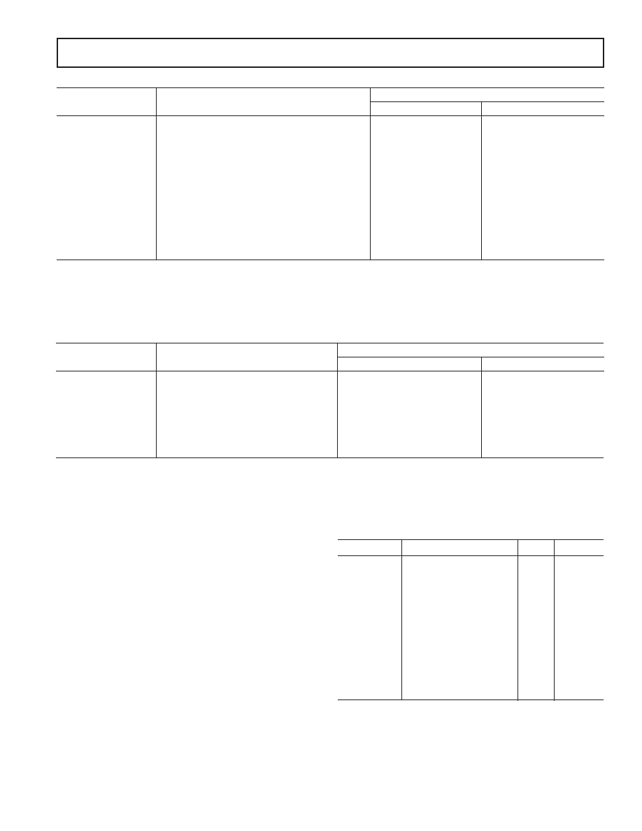
Table I. Ideal Code Transition Table for the AD7891-1,
10 V and
5 V Ranges and the AD7891-2,
2.5 V Range
Digital Output Code Transition
1
Analog Input
Input Voltage
Twos Complement
Straight Binary
+FSR
2/2 – 3/2 LSB3
(9.99268 V, 4.99634 V or 2.49817 V)
4
011...110 to 011...111
111...110 to 111...111
+FSR/2 – 5/2 LSB
(9.98779 V, 4.99390 V or 2.49695 V)
011...101 to 011...110
111...101 to 111...110
+FSR/2 – 7/2 LSB
(9.99145 V, 4.99146 V or 2.49573 V)
011...100 to 011...101
111...100 to 111...101
AGND + 3/2 LSB
(7.3242 mV, 3.6621 mV or 1.8310 mV)
000...001 to 000...010
100...001 to 100...010
AGND + 1/2 LSB
(2.4414 mV, 1.2207 mV or 0.6103 mV)
000...000 to 000...001
100...000 to 100...001
AGND – 1/2 LSB
(–2.4414 mV, –1.2207 mV or –0.6103 mV)
111...111 to 000...000
011...111 to 100...000
AGND – 3/2 LSB
(–7.3242 mV, –3.6621 mV or –1.8310 mV)
111...110 to 111...111
011...110 to 011...111
–FSR/2 + 5/2 LSB
(–9.98779 V, –4.99390 V or –2.49695 V)
100...010 to 100...011
000...010 to 000...011
–FSR/2 + 3/2 LSB
(–9.99268 V, –4.99634 V or –2.49817 V)
100...001 to 100...010
000...001 to 000...010
–FSR/2 + 1/2 LSB
(–9.99756 V, –4.99878 V or –2.49939 V)
100...000 to 100...001
000...000 to 000...001
NOTES
1Output code format is determined by the FORMAT bit in the control register.
2FSR is full-scale range and is +20 V for the
±10 V range, +10 V for the ±5 V range, and +5 V for the ±2.5 V range, with REF IN = +2.5 V.
31 LSB = FSR/4096 = +4.88 mV (
±10 V range), +2.44 mV (±5 V range), and +1.22 mV (±2.5 V range), with REF IN = +2.5 V.
4
±10 V range, ±5 V range, or ±2.5 V range.
Table II. Ideal Code Transition Table for the AD7891-2, 0 V to 5 V and 0 V to 2.5 V Ranges
Digital Output Code Transition
1
Analog Input
Input Voltage
Twos Complement
Straight Binary
+FSR
2 – 3/2 LSB3
(4.99817 V or 2.49908 V)
4
011...110 to 011...111
111...110 to 111...111
+FSR – 5/2 LSB
(4.99695 V or 2.49847 V)
011...101 to 011...110
111...101 to 111...110
+FSR – 7/2 LSB
(4.99573 V or 2.49786 V)
011...100 to 011...101
111...100 to 111...101
AGND + 5/2 LSB
(3.0518 mV or 1.52588 mV)
100...010 to 000...011
000...010 to 000...011
AGND + 3/2 LSB
(1.83105 mV or 0.9155 mV)
100...001 to 000...010
000...001 to 000...010
AGND + 1/2 LSB
(0.6103 mV or 0.3052 mV)
100...000 to 000...001
000...000 to 000...001
NOTES
1Output code format is determined by the FORMAT bit in the control register.
2FSR is the full-scale range and is 5 V for the 0 to 5 V range and 2.5 V for the 0 to 2.5 V range, with REF IN = 2.5 V.
31 LSB = F
S/4096 = 1.22 mV (0 to 5 V range) or 610
mV (0 to 2.5 V range), with REF IN = 2.5 V.
40 V to 5 V range or 0 V to 2.5 V range.
Table III. Transfer Function M and N Values
Range
Output Data Format
M
N
AD7891-1
±10 V
Straight Binary
8
–4
±10 V
Twos Complement
8
0
±5 V
Straight Binary
4
–2
±5 V
Twos Complement
4
0
AD7891-2
0 V to +5 V
Straight Binary
2
0
0 V to +5 V
Twos Complement
2
1
0 V to +2.5 V
Straight Binary
1
0
0 V to +2.5 V
Twos Complement
1
0.5
±2.5 V
Straight Binary
2
–1
±2.5 V
Twos Complement
2
0
Transfer Function of the AD7891-1 and AD7891-2
The transfer function of the AD7891-1 and AD7891-2 can be
expressed as
Input Voltage
M
REF IN
D
N
REF IN
=
() +
()
/4096
D is the output data from the AD7891 and is in the range 0 to
4095 for straight binary encoding and from –2048 to +2047 for
twos complement encoding. Values for M depend upon the
input voltage range. Values for N depend upon the input voltage
range and the output data format. These values are given in
Table III. REF IN is the reference voltage applied to the AD7891.
相关PDF资料 |
PDF描述 |
|---|---|
| LTC6906IS6#TRMPBF | IC OSC SILICON 1MHZ TSOT23-6 |
| AD7891YSZ-2 | IC DAS 12BIT 8CH 44-MQFP |
| LTC6907IS6#TRPBF | IC OSC SILICON 4MHZ TSOT23-6 |
| LTC6906IS6#TRPBF | IC OSC SILICON 1MHZ TSOT23-6 |
| AD974AN | IC DAS 16BIT 4CH 200KSPS 28-DIP |
相关代理商/技术参数 |
参数描述 |
|---|---|
| AD7891YPZ-1REEL | 功能描述:IC DAS 12BIT 8CH 44-PLCC RoHS:是 类别:集成电路 (IC) >> 数据采集 - ADCs/DAC - 专用型 系列:- 产品培训模块:Lead (SnPb) Finish for COTS Obsolescence Mitigation Program 标准包装:50 系列:- 类型:数据采集系统(DAS) 分辨率(位):16 b 采样率(每秒):21.94k 数据接口:MICROWIRE?,QSPI?,串行,SPI? 电压电源:模拟和数字 电源电压:1.8 V ~ 3.6 V 工作温度:-40°C ~ 85°C 安装类型:表面贴装 封装/外壳:40-WFQFN 裸露焊盘 供应商设备封装:40-TQFN-EP(6x6) 包装:托盘 |
| AD7891YS1 | 制造商:AD 功能描述:New |
| AD7891YS-1 | 制造商:Analog Devices 功能描述:ADC Single 454.5ksps 12-bit Parallel/Serial 44-Pin MQFP |
| AD7891YS-1REEL | 制造商:Analog Devices 功能描述:ADC Single 454.5ksps 12-bit Parallel/Serial 44-Pin MQFP T/R 制造商:Analog Devices 功能描述:ADC SGL 454.5KSPS 12-BIT PARALLEL/SERL 44MQFP - Tape and Reel |
| AD7891YS-2 | 制造商:Analog Devices 功能描述:ADC Single 500ksps 12-bit Parallel/Serial 44-Pin MQFP 制造商:Rochester Electronics LLC 功能描述:8 CHANNEL, 12-BIT ADC I.C. - Bulk |
发布紧急采购,3分钟左右您将得到回复。