参数资料
| 型号: | AD7891YPZ-1 |
| 厂商: | Analog Devices Inc |
| 文件页数: | 3/20页 |
| 文件大小: | 0K |
| 描述: | IC DAS 12BIT 8CH 44-PLCC |
| 标准包装: | 1 |
| 类型: | 数据采集系统(DAS) |
| 分辨率(位): | 12 b |
| 采样率(每秒): | 500k |
| 数据接口: | 串行,并联 |
| 电压电源: | 单电源 |
| 电源电压: | 5V |
| 工作温度: | -55°C ~ 105°C |
| 安装类型: | 表面贴装 |
| 封装/外壳: | 44-LCC(J 形引线) |
| 供应商设备封装: | 44-PLCC(16.59x16.59) |
| 包装: | 管件 |
AD7891
–11–
REV. D
Serial Interface Mode
The serial interface mode is selected by tying the MODE input
to a logic low. In this case, five of the data/control inputs of the
parallel mode assume serial interface functions.
The serial interface on the AD7891 is a 5-wire interface with
read and write capabilities, with data being read from the output
register via the DATA OUT line and data being written to the
control register via the DATA IN line. The part operates in a
slave or external clocking mode and requires an externally applied
serial clock to the SCLK input to access data from the data
register or write data to the control register. There are separate
framing signals for the read (
RFS) and write (TFS) operations.
The serial interface on the AD7891 is designed to allow the part
to be interfaced to systems that provide a serial clock that is
synchronized to the serial data, such as the 80C51, 87C51,
68HC11, and 68HC05, and most digital signal processors.
When using the AD7891 in serial mode, the data lines DB11 to
DB10 should be tied to logic low, and the
CS, WR, and RD
inputs should be tied to logic high. Pins DB4 to DB0 can be
tied to either logic high or logic low but must not be left floating
because this condition could cause the AD7891 to draw
large amounts of current.
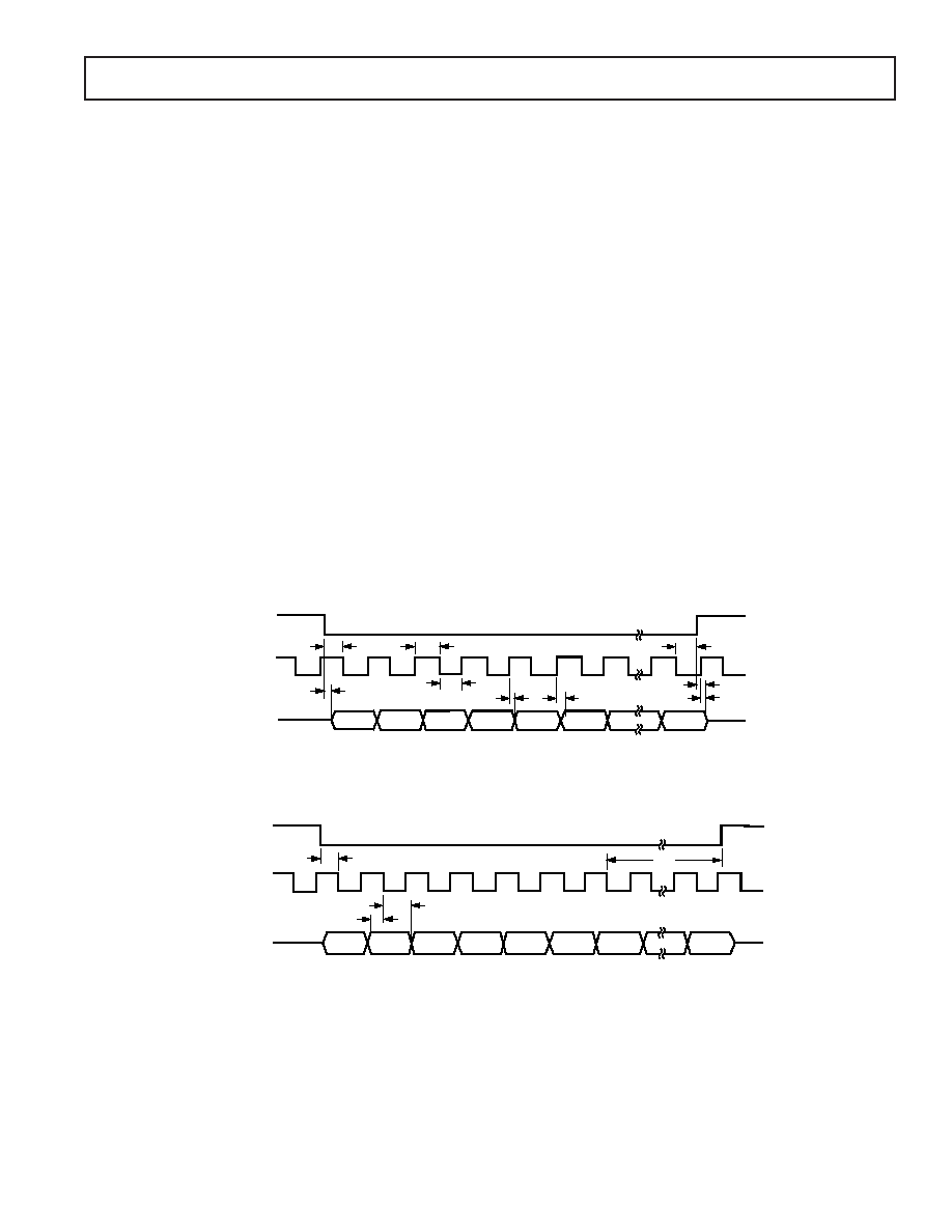
Read Operation
Figure 3 shows the timing diagram for reading from the AD7891
in serial mode.
RFS goes low to access data from the AD7891.
The serial clock input does not have to be continuous. The serial
data can be accessed in a number of bytes. However,
RFS must
remain low for the duration of the data transfer operation. Six-
teen bits of data are transmitted in serial mode with the data
FORMAT bit first, followed by the three address bits in the
control register, followed by the 12-bit conversion result starting
with the MSB. Serial data is clocked out of the device on the
rising edge of SCLK and is valid on the falling edge of SCLK.
At the end of the read operation, the DATA OUT line is three-
stated by a rising edge on either the SCLK or
RFS inputs, which-
ever occurs first.
Write Operation
Figure 4 shows a write operation to the control register of the
AD7891. The
TFS input goes low to indicate to the part that a
serial write is about to occur. The AD7891 control register
requires only six bits of data. These are loaded on the first six
clock cycles of the serial clock with data on all subsequent clock
cycles being ignored. Serial data to be written to the AD7891
must be valid on the falling edge of SCLK.
Simplifying the Serial Interface
To minimize the number of interconnect lines to the AD7891
in serial mode, the user can connect the
RFS and TFS lines
of the AD7891 together and read and write from the part simul-
taneously. In this case, a new control register data line selecting
the input channel and providing a conversion start command
should be provided on the DATA IN line, while the part pro-
vides the result from the conversion just completed on the
DATA OUT line.
DATA OUT (O)
SCLK (I)
RFS (I)
t18A
NOTE
I = INPUT
O = OUTPUT
FORMAT
A2
A1
A0
DB11
DB10
DB0
THREE-STATE
t18
t16
t15
t14
t12
t11
t13
t17
Figure 3. Serial Mode Read Operation
DATA IN (I)
SCLK (I)
TFS (I)
NOTE
I = INPUT
FORMAT
A0
A1
A0
t19
t22
t21
t20
CONV
STBY
DON'T
CARE
DON'T
CARE
Figure 4. Serial Mode Write Operation
相关PDF资料 |
PDF描述 |
|---|---|
| LTC6906IS6#TRMPBF | IC OSC SILICON 1MHZ TSOT23-6 |
| AD7891YSZ-2 | IC DAS 12BIT 8CH 44-MQFP |
| LTC6907IS6#TRPBF | IC OSC SILICON 4MHZ TSOT23-6 |
| LTC6906IS6#TRPBF | IC OSC SILICON 1MHZ TSOT23-6 |
| AD974AN | IC DAS 16BIT 4CH 200KSPS 28-DIP |
相关代理商/技术参数 |
参数描述 |
|---|---|
| AD7891YPZ-1REEL | 功能描述:IC DAS 12BIT 8CH 44-PLCC RoHS:是 类别:集成电路 (IC) >> 数据采集 - ADCs/DAC - 专用型 系列:- 产品培训模块:Lead (SnPb) Finish for COTS Obsolescence Mitigation Program 标准包装:50 系列:- 类型:数据采集系统(DAS) 分辨率(位):16 b 采样率(每秒):21.94k 数据接口:MICROWIRE?,QSPI?,串行,SPI? 电压电源:模拟和数字 电源电压:1.8 V ~ 3.6 V 工作温度:-40°C ~ 85°C 安装类型:表面贴装 封装/外壳:40-WFQFN 裸露焊盘 供应商设备封装:40-TQFN-EP(6x6) 包装:托盘 |
| AD7891YS1 | 制造商:AD 功能描述:New |
| AD7891YS-1 | 制造商:Analog Devices 功能描述:ADC Single 454.5ksps 12-bit Parallel/Serial 44-Pin MQFP |
| AD7891YS-1REEL | 制造商:Analog Devices 功能描述:ADC Single 454.5ksps 12-bit Parallel/Serial 44-Pin MQFP T/R 制造商:Analog Devices 功能描述:ADC SGL 454.5KSPS 12-BIT PARALLEL/SERL 44MQFP - Tape and Reel |
| AD7891YS-2 | 制造商:Analog Devices 功能描述:ADC Single 500ksps 12-bit Parallel/Serial 44-Pin MQFP 制造商:Rochester Electronics LLC 功能描述:8 CHANNEL, 12-BIT ADC I.C. - Bulk |
发布紧急采购,3分钟左右您将得到回复。