参数资料
| 型号: | AD8155ACPZ |
| 厂商: | Analog Devices Inc |
| 文件页数: | 15/36页 |
| 文件大小: | 0K |
| 描述: | IC MUX/DEMUX DUAL BUFFER 64LFCSP |
| 标准包装: | 1 |
| 系列: | XStream™ |
| 功能: | 多路复用器/多路分解器 |
| 电路: | 2 x 2:1 |
| 电压电源: | 单电源 |
| 电压 - 电源,单路/双路(±): | 1.6 V ~ 3.6 V |
| 电流 - 电源: | 735mA |
| 工作温度: | -40°C ~ 85°C |
| 安装类型: | 表面贴装 |
| 封装/外壳: | 64-VFQFN 裸露焊盘,CSP |
| 供应商设备封装: | 64-LFCSP-VQ(9x9) |
| 包装: | 托盘 |
第1页第2页第3页第4页第5页第6页第7页第8页第9页第10页第11页第12页第13页第14页当前第15页第16页第17页第18页第19页第20页第21页第22页第23页第24页第25页第26页第27页第28页第29页第30页第31页第32页第33页第34页第35页第36页
AD8155
Rev. 0 | Page 22 of 36
The final section is the outputs section. For an individual
output, the programmed output current flows through two
separate paths. One is the on-chip termination resistor, and the
other is the transmission line and the destination termination
resistor. The nominal parallel impedance of these two paths is
25 Ω. The sum of these two currents flows through the switches
and the current source of the AD8155 output circuit and out
through VEE. The power dissipated in the transmission line and the
destination resistor is not dissipated in the AD8155 but must be
supplied from the power supply and is a factor in overall system
power. The current in the on-chip termination resistors and the
output current source dissipate power in the AD8155 itself.
frequency of maximum boost without sacrificing the amount of
boost delivered.
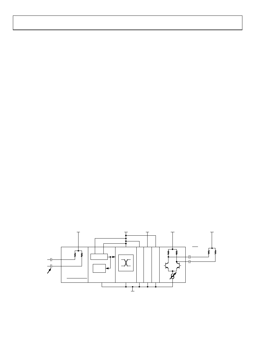
AD8155 POWER CONSUMPTION
There are several sections of the AD8155 that draw varying
power depending on the supply voltages, the type of I/O coupling
used, and the status of the AD8155 operation. Figure 40 shows a
block diagram of these sections. An initialization sequence is
required to enable the AD8155 in a low power mode (see the
Applications Information section).
The first section consists of the input termination resistors. The
power dissipated in the termination resistors is due to the input
differential swing and any common-mode current resulting
from dc-coupling the input.
Outputs
The output current is set by a combination of output level and
preemphasis settings (see Table 19). For the two logic switch
states, this current flows through an on-chip termination
resistor and a parallel path to the destination device and its
termination resistor. The power in this parallel path is not
dissipated by the AD8155. With preemphasis enabled, some
current always flows in both the P and N termination resistors.
This preemphasis current gives rise to an output common-
mode shift, which varies with ac-coupling or dc-coupling and
which is calculated for both cases in Table 19.
In the next section (the receiver section), each input is powered
only when it is selected, and the disable bits are set to 0. If a
receiver is not selected, it is powered down. Thus, the total
number of active inputs affects the total power consumption.
Furthermore, the loss-of-signal detection circuits can be
disabled independent of the receiver for even greater power
savings.
The core of the device performs the multiplexer and demulti-
plexer switching functions. It draws a fixed quiescent current of
2 mA whenever the AD8155 is powered from VCC to VEE. The
switch draws an additional 4 × 4.6 mA in normal mux/demux
operation and an additional 6 × 4.6 mA with all ports in loop-
back or with bicast selected. The switch core can be disabled to
save power.
Perhaps the most direct method for calculating power dissi-
pated in the output is to calculate the power that would be
dissipated if all of ITOT were to flow on-die from VTTO to VEE
and to subtract from this the power dissipated off die in the
destination device termination resistors and the channel.
For this purpose, the destination device and channel can be
modeled as 50 Ω load resistors, RL, in parallel with the AD8155
termination resistors.
An output predriver section draws a current, IPRED, that is
related to the programmed output current, ITTO. The predriver
current always flows from VCC to VEE. It is treated separately
from the output current, which flows from VTTO and may not be
the same voltage as VCC.
.
IP_xx
IN_xx
VTTI
VEE
AC-COUPLING CAPS
(OPTIONAL)
INPUT
TERMINATION
P =
(VIN_DIFF_RMS)2
100
EQUALIZER
RECEIVER
SWITCH
RE
F
E
R
E
NCE
S
/
BI
AS
C
IR
CUI
T
R
Y
DI
G
IT
A
L
CO
NT
R
O
L
OU
TP
U
T
P
R
ED
R
IVER
S
LOSS OF
SIGNAL
50
VTTO
IOUT
VTT
V
50
OUTPUT
TERMINATIONS
P =
× 50
IOUT
2
OPTIONAL COUPLING
CAPACITORS
P = (VOL) (IOUT)
VOL = VTTO – (IOUT × 25)
CC
DVCC
08
26
2-
0
41
Figure 40. AD8155 Power Distribution Block Diagram
相关PDF资料 |
PDF描述 |
|---|---|
| AD8156ABCZ | IC SWITCH XPT 4X4 W/EQ 49CSPBGA |
| AD8158ACPZ | IC MUX/DEMUX QUAD 2X1 100LFCSP |
| AD8159ASVZ | IC MUX/DEMUX QUAD BUFF 100TQFP |
| AD8174ANZ | IC MUX SW W/AMP 250MHZ 14-DIP |
| AD8175ABPZ | IC CROSSPOINT SWITCH TRPL 676BGA |
相关代理商/技术参数 |
参数描述 |
|---|---|
| AD8155ACPZ-R7 | 功能描述:IC MUX/DEMUX DUAL BUFFER 64LFCSP RoHS:是 类别:集成电路 (IC) >> 接口 - 模拟开关,多路复用器,多路分解器 系列:XStream™ 其它有关文件:STG4159 View All Specifications 标准包装:5,000 系列:- 功能:开关 电路:1 x SPDT 导通状态电阻:300 毫欧 电压电源:双电源 电压 - 电源,单路/双路(±):±1.65 V ~ 4.8 V 电流 - 电源:50nA 工作温度:-40°C ~ 85°C 安装类型:表面贴装 封装/外壳:7-WFBGA,FCBGA 供应商设备封装:7-覆晶 包装:带卷 (TR) |
| AD8155-EVALZ | 制造商:AD 制造商全称:Analog Devices 功能描述:6.5 Gbps Dual Buffer Mux/Demux |
| AD8155XCPZ | 制造商:Analog Devices 功能描述: |
| AD8156 | 制造商:AD 制造商全称:Analog Devices 功能描述:6.25 Gbps 4】4 Digital Crosspoint Switch with EQ |
| AD8156ABCZ | 功能描述:IC SWITCH XPT 4X4 W/EQ 49CSPBGA RoHS:是 类别:集成电路 (IC) >> 接口 - 专用 系列:XStream™ 特色产品:NXP - I2C Interface 标准包装:1 系列:- 应用:2 通道 I²C 多路复用器 接口:I²C,SM 总线 电源电压:2.3 V ~ 5.5 V 封装/外壳:16-TSSOP(0.173",4.40mm 宽) 供应商设备封装:16-TSSOP 包装:剪切带 (CT) 安装类型:表面贴装 产品目录页面:825 (CN2011-ZH PDF) 其它名称:568-1854-1 |
发布紧急采购,3分钟左右您将得到回复。