参数资料
| 型号: | AD8155ACPZ |
| 厂商: | Analog Devices Inc |
| 文件页数: | 17/36页 |
| 文件大小: | 0K |
| 描述: | IC MUX/DEMUX DUAL BUFFER 64LFCSP |
| 标准包装: | 1 |
| 系列: | XStream™ |
| 功能: | 多路复用器/多路分解器 |
| 电路: | 2 x 2:1 |
| 电压电源: | 单电源 |
| 电压 - 电源,单路/双路(±): | 1.6 V ~ 3.6 V |
| 电流 - 电源: | 735mA |
| 工作温度: | -40°C ~ 85°C |
| 安装类型: | 表面贴装 |
| 封装/外壳: | 64-VFQFN 裸露焊盘,CSP |
| 供应商设备封装: | 64-LFCSP-VQ(9x9) |
| 包装: | 托盘 |
第1页第2页第3页第4页第5页第6页第7页第8页第9页第10页第11页第12页第13页第14页第15页第16页当前第17页第18页第19页第20页第21页第22页第23页第24页第25页第26页第27页第28页第29页第30页第31页第32页第33页第34页第35页第36页
AD8155
Rev. 0 | Page 24 of 36
I2C CONTROL INTERFACE
SERIAL INTERFACE GENERAL FUNCTIONALITY
The AD8155 register set is controlled through a 2-wire I2C
interface. The AD8155 acts only as an I2C slave device. The
7-bit slave address for the AD8155 I2C interface contains the
static value b1010 for the upper four bits. The lower three bits
are controlled by the input pins, I2C_A[2:0].
Therefore, the I2C bus in the system must include an I2C master
to configure the AD8155 and other I2C devices that may be on
the bus. Data transfers are controlled through the use of the two
I2C wires: the SCL input clock pin and the SDA bidirectional
data pin.
The AD8155 I2C interface can be run in the standard (64 kHz)
and fast (400 kHz) modes. The SDA line changes value only
when the SCL pin is low, with two exceptions. To indicate the
beginning or continuation of a transfer, the SDA pin is driven
low while the SCL pin is high, and to indicate the end of a
transfer, the SDA line is driven high while the SCL line is high.
Therefore, it is important to control the SCL clock to toggle
only when the SDA line is stable unless indicating a start,
repeated start, or stop condition.
I2C INTERFACE DATA TRANSFERS: DATA WRITE
To write data to the AD8155 register set, a microcontroller or
any other I2C master must send the appropriate control signals
to the AD8155 slave device. The following steps must be taken,
where the signals are controlled by the I2C master, unless other-
wise specified. For a diagram of the procedure, see Figure 41.
1.
Send a start condition (while holding the SCL line high,
pull the SDA line low).
2.
Send the AD8155 part address (seven bits) whose upper
four bits are the static value b1010 and whose lower three
bits are controlled by the I2C_A[2:0] input pins. This
transfer should be MSB first.
3.
Send the write indicator bit (0).
4.
Wait for the AD8155 to acknowledge the request.
5.
Send the register address (eight bits) to which data is to be
written. This transfer should be MSB first.
6.
Wait for the AD8155 to acknowledge the request.
7.
Send the data (eight bits) to be written to the register whose
address was set in Step 5. This transfer should be MSB first.
8.
Wait for the AD8155 to acknowledge the request.
9.
Do one or more of the following:
a.
Send a stop condition (while holding the SCL line
high, pull the SDA line high) and release control of
the bus.
b.
Send a repeated start condition (while holding the
SCL line high, pull the SDA line low) and continue
with Step 2 in this procedure to perform another write.
c.
Send a repeated start condition (while holding the
SCL line high, pull the SDA line low) and continue
with Step 2 of the read procedure (in the I2C Interface
Data Transfers: Data Read section) to perform a read
from another address.
d.
Send a repeated start condition (while holding the
SCL line high, pull the SDA line low) and continue
with Step 8 of the read procedure (in the I2C Interface
Data Transfers: Data Read section) to perform a read
from the same address set in Step 5.
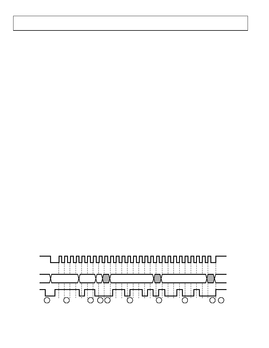
In Figure 41, the AD8155 write process is shown. The SCL
signal is shown along with a general write operation and a
specific example. In this example, the value 0x92 is written to
Address 0x6D of an AD8155 device with a part address of 0x53.
The part address is seven bits wide and is composed of the
AD8155 static upper four bits (b1010) and the pin-programmable
lower three bits (I2C_A[2:0]). The address pins are set to b011.
In Figure 41, the corresponding step number is visible in the
circle under the waveform. The SCL line is driven by the I2C
master and never by the AD8155 slave. As for the SDA line, the
data in the shaded polygons is driven by the AD8155, whereas
the data in the nonshaded polygons is driven by the I2C master.
The end phase case shown is that of Step 9a.
It is important to note that the SDA line changes only when the
SCL line is low, except for the case of sending a start, stop, or
repeated start condition (Step 1 and Step 9 in this case).
START
R/W ACK
ACK
STOP
DATA
ADDR
[2:0]
b1010
REGISTER ADDR
SCL
SDA
1
2
3
4
5
6
7
9a
0
826
2-
0
42
8
Figure 41. I2C Write Diagram
相关PDF资料 |
PDF描述 |
|---|---|
| AD8156ABCZ | IC SWITCH XPT 4X4 W/EQ 49CSPBGA |
| AD8158ACPZ | IC MUX/DEMUX QUAD 2X1 100LFCSP |
| AD8159ASVZ | IC MUX/DEMUX QUAD BUFF 100TQFP |
| AD8174ANZ | IC MUX SW W/AMP 250MHZ 14-DIP |
| AD8175ABPZ | IC CROSSPOINT SWITCH TRPL 676BGA |
相关代理商/技术参数 |
参数描述 |
|---|---|
| AD8155ACPZ-R7 | 功能描述:IC MUX/DEMUX DUAL BUFFER 64LFCSP RoHS:是 类别:集成电路 (IC) >> 接口 - 模拟开关,多路复用器,多路分解器 系列:XStream™ 其它有关文件:STG4159 View All Specifications 标准包装:5,000 系列:- 功能:开关 电路:1 x SPDT 导通状态电阻:300 毫欧 电压电源:双电源 电压 - 电源,单路/双路(±):±1.65 V ~ 4.8 V 电流 - 电源:50nA 工作温度:-40°C ~ 85°C 安装类型:表面贴装 封装/外壳:7-WFBGA,FCBGA 供应商设备封装:7-覆晶 包装:带卷 (TR) |
| AD8155-EVALZ | 制造商:AD 制造商全称:Analog Devices 功能描述:6.5 Gbps Dual Buffer Mux/Demux |
| AD8155XCPZ | 制造商:Analog Devices 功能描述: |
| AD8156 | 制造商:AD 制造商全称:Analog Devices 功能描述:6.25 Gbps 4】4 Digital Crosspoint Switch with EQ |
| AD8156ABCZ | 功能描述:IC SWITCH XPT 4X4 W/EQ 49CSPBGA RoHS:是 类别:集成电路 (IC) >> 接口 - 专用 系列:XStream™ 特色产品:NXP - I2C Interface 标准包装:1 系列:- 应用:2 通道 I²C 多路复用器 接口:I²C,SM 总线 电源电压:2.3 V ~ 5.5 V 封装/外壳:16-TSSOP(0.173",4.40mm 宽) 供应商设备封装:16-TSSOP 包装:剪切带 (CT) 安装类型:表面贴装 产品目录页面:825 (CN2011-ZH PDF) 其它名称:568-1854-1 |
发布紧急采购,3分钟左右您将得到回复。