- 您现在的位置:买卖IC网 > PDF目录16848 > AD9523-1/PCBZ (Analog Devices Inc)BOARD EVAL FOR AD9523-1 PDF资料下载
参数资料
| 型号: | AD9523-1/PCBZ |
| 厂商: | Analog Devices Inc |
| 文件页数: | 14/60页 |
| 文件大小: | 0K |
| 描述: | BOARD EVAL FOR AD9523-1 |
| 设计资源: | AD9523(-1) Eval Board Schematic AD9523(-1) BOM AD9523(-1) Gerber Files |
| 标准包装: | 1 |
| 主要目的: | 计时,时钟发生器 |
| 嵌入式: | 否 |
| 已用 IC / 零件: | AD9523 |
| 主要属性: | 板载 PLL 环路滤波器 |
| 次要属性: | LED 状态指示器 |
| 已供物品: | 板 |
第1页第2页第3页第4页第5页第6页第7页第8页第9页第10页第11页第12页第13页当前第14页第15页第16页第17页第18页第19页第20页第21页第22页第23页第24页第25页第26页第27页第28页第29页第30页第31页第32页第33页第34页第35页第36页第37页第38页第39页第40页第41页第42页第43页第44页第45页第46页第47页第48页第49页第50页第51页第52页第53页第54页第55页第56页第57页第58页第59页第60页
AD9523-1
Rev. B | Page 21 of 60
THEORY OF OPERATION
DETAILED BLOCK DIAGRAM
CHARGE
PUMP
VCXO
SWITCH-
OVER
CONTROL
M2
OUT13
OUT12
OUT11
OUT10
OUT9
OUT8
OUT7
OUT6
OUT5
OUT4
OUT3
OUT2
OUT1
OUT0
OUT13
OUT12
OUT11
OUT10
OUT9
OUT8
OUT7
OUT6
OUT5
OUT4
OUT3
OUT2
OUT1
OUT0
STATUS MONITOR
LOCK DETECT/
SERIAL PORT
ADDRESS
CONTROL
INTERFACE
(SDI AND I2C)
SCLK/SCL
SDO
SDIO/SDA
÷N2
PLL2
(T
ES
T
PA
T
H
)
LDO_DIV_MI
LOOP
FILTER
LOOP
FILTER
CHARGE
PUMP
PLL1
LOCK
DETECT
LOCK
DETECT
P
F
D
ZD_IN
PD
RESET
SYNC
÷D
t
EDGE
SELECT
÷D
t
EDGE
SELECT
÷D
t
EDGE
SELECT
÷D
FANOUT
t
EDGE
SELECT
t
EDGE
SELECT
t
EDGE
SELECT
t
EDGE
SELECT
t
EDGE
SELECT
t
EDGE
SELECT
t
EDGE
SELECT
÷D
t
EDGE
SELECT
÷D
t
EDGE
SELECT
÷D
t
EDGE
SELECT
÷D
t
EDGE
SELECT
PLL1_OUT
VDD1.8_OUT[x:y]
REFA
REFB
AD9523-1
REF_SEL
STATUS0/
SP0
STATUS1/
SP1
EEPROM
EEPROM_SEL
LF2_EXT_CAP
LF1_EXT_CAP
REF_TEST
OSC_CTRL
OSC_IN
CS
÷R1
÷N1
LDO_PLL1
LDO_VCO
VDD3_OUT[x:y]
VDD3_PLL
VDD3_VCO
VCO
P
F
D
÷R1
0
9278-
02
0
÷D1
÷R2
×2
M1
FANOUT
÷D
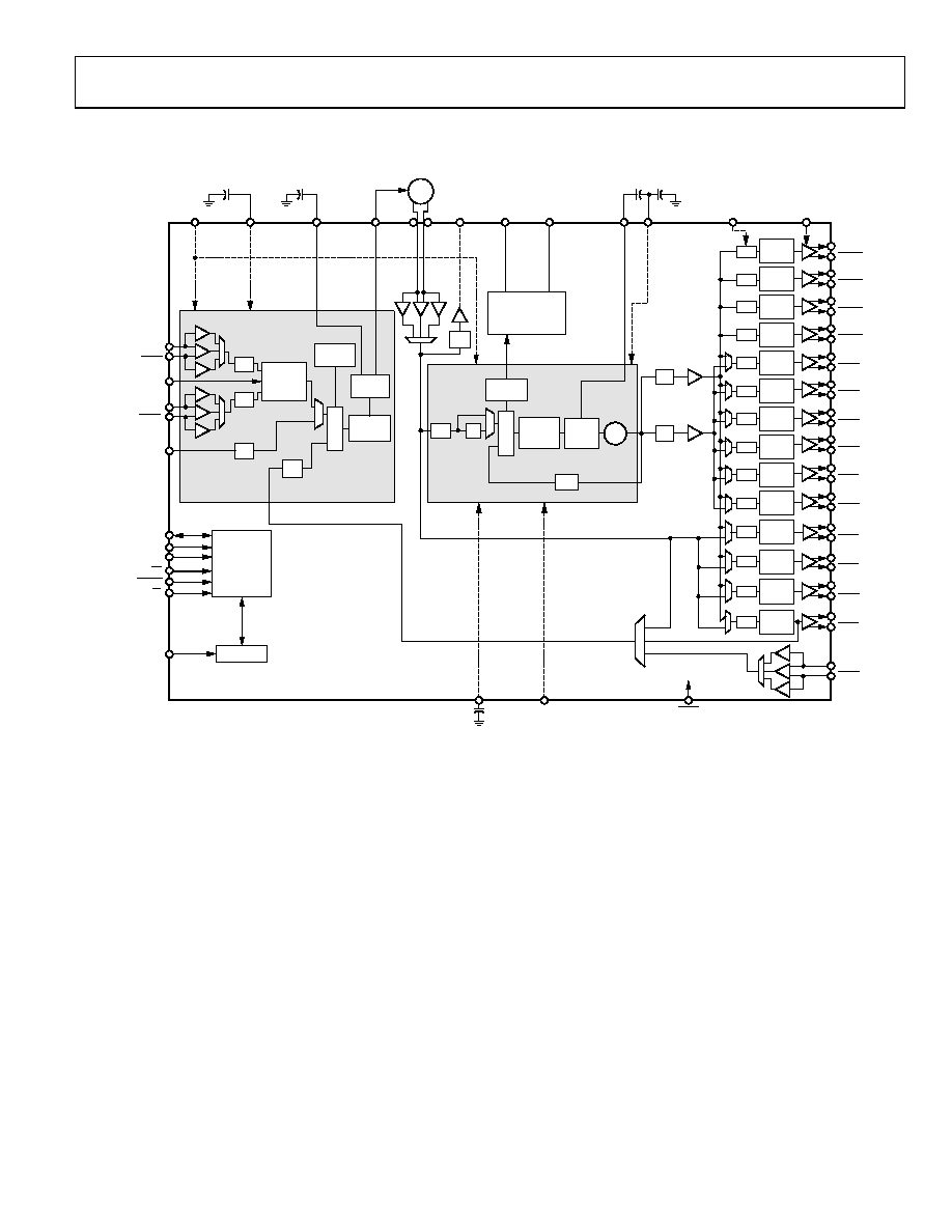
Figure 24. Top Level Diagram
OVERVIEW
The AD9523-1 is a clock generator that employs integer-N-based
phase-locked loops (PLL). The device architecture consists of two
cascaded PLL stages. The first stage, PLL1, consists of an integer
division PLL that uses an external voltage-controlled crystal
oscillator (VCXO) from 15 MHz to 250 MHz. PLL1 has a narrow-
loop bandwidth that provides initial jitter cleanup of the input
reference signal. The second stage, PLL2, is a frequency
multiplying PLL that translates the first stage output frequency
to a range of 2.94 GHz to 2.96 GHz. PLL2 incorporates an
integer-based feedback divider that enables integer frequency
multiplication. Programmable integer dividers (1 to 1024) follow
PLL2, establishing a final output frequency of 1 GHz or less.
The AD9523-1 includes reference signal processing blocks that
enable a smooth switching transition between two reference inputs.
This circuitry automatically detects the presence of the reference
input signals. If only one input is present, the device uses it as
the active reference. If both are present, one becomes the active
reference and the other becomes the backup reference. If the active
reference fails, the circuitry automatically switches to the backup
reference (if available), making it the new active reference.
A register setting determines what action to take if the failed
reference is once again available: either stay on Reference B or
revert to Reference A. If neither reference is usable, the AD9523-1
supports a holdover mode. A reference select pin (REF_SEL,
Pin 16) is available to manually select which input reference is
active (see Table 42). The accuracy of the holdover is dependent
on the external VCXO frequency stability at half supply voltage.
Any of the divider settings are programmable via the serial
programming port, enabling a wide range of input/output
frequency ratios under program control. The dividers also
include a programmable delay to adjust timing of the output
signals, if required.
The output is compatible with LVPECL, LVDS, or HSTL logic
levels (see the Input/Output Termination Recommendations
section); however, the AD9523-1 is implemented only in CMOS.
The loop filters of each PLL are integrated and programmable.
Only a single external capacitor for each of the two PLL loop
filters is required.
The AD9523-1 operates over the extended industrial temperature
range of 40°C to +85°C.
相关PDF资料 |
PDF描述 |
|---|---|
| V150C5C100BF | CONVERTER MOD DC/DC 5V 100W |
| V150C5C100BL3 | CONVERTER MOD DC/DC 5V 100W |
| V150C5C100B3 | CONVERTER MOD DC/DC 5V 100W |
| V150C5C100B2 | CONVERTER MOD DC/DC 5V 100W |
| AD9512/PCBZ | BOARD EVAL FOR AD9512 |
相关代理商/技术参数 |
参数描述 |
|---|---|
| AD9523BCPZ | 功能描述:IC INTEGER-N CLCK GEN 72LFCSP RoHS:是 类别:集成电路 (IC) >> 时钟/计时 - 专用 系列:- 标准包装:28 系列:- 类型:时钟/频率发生器 PLL:是 主要目的:Intel CPU 服务器 输入:时钟 输出:LVCMOS 电路数:1 比率 - 输入:输出:3:22 差分 - 输入:输出:无/是 频率 - 最大:400MHz 电源电压:3.135 V ~ 3.465 V 工作温度:0°C ~ 85°C 安装类型:表面贴装 封装/外壳:64-TFSOP (0.240",6.10mm 宽) 供应商设备封装:64-TSSOP 包装:管件 |
| AD9523BCPZ-REEL7 | 功能描述:IC INTEGER-N CLCK GEN 72LFCSP RoHS:是 类别:集成电路 (IC) >> 时钟/计时 - 专用 系列:- 标准包装:28 系列:- 类型:时钟/频率发生器 PLL:是 主要目的:Intel CPU 服务器 输入:时钟 输出:LVCMOS 电路数:1 比率 - 输入:输出:3:22 差分 - 输入:输出:无/是 频率 - 最大:400MHz 电源电压:3.135 V ~ 3.465 V 工作温度:0°C ~ 85°C 安装类型:表面贴装 封装/外壳:64-TFSOP (0.240",6.10mm 宽) 供应商设备封装:64-TSSOP 包装:管件 |
| AD9524 | 制造商:AD 制造商全称:Analog Devices 功能描述:Jitter Cleaner and Clock Generator with 6 Differential or 13 LVCMOS Outputs |
| AD9524/PCBZ | 功能描述:BOARD EVAL FOR AD9524 RoHS:是 类别:编程器,开发系统 >> 评估演示板和套件 系列:- 标准包装:1 系列:PSoC® 主要目的:电源管理,热管理 嵌入式:- 已用 IC / 零件:- 主要属性:- 次要属性:- 已供物品:板,CD,电源 |
| AD9524BCPZ | 功能描述:IC INTEGER-N CLCK GEN 48LFCSP RoHS:是 类别:集成电路 (IC) >> 时钟/计时 - 专用 系列:- 标准包装:28 系列:- 类型:时钟/频率发生器 PLL:是 主要目的:Intel CPU 服务器 输入:时钟 输出:LVCMOS 电路数:1 比率 - 输入:输出:3:22 差分 - 输入:输出:无/是 频率 - 最大:400MHz 电源电压:3.135 V ~ 3.465 V 工作温度:0°C ~ 85°C 安装类型:表面贴装 封装/外壳:64-TFSOP (0.240",6.10mm 宽) 供应商设备封装:64-TSSOP 包装:管件 |
发布紧急采购,3分钟左右您将得到回复。