- 您现在的位置:买卖IC网 > PDF目录16848 > AD9523-1/PCBZ (Analog Devices Inc)BOARD EVAL FOR AD9523-1 PDF资料下载
参数资料
| 型号: | AD9523-1/PCBZ |
| 厂商: | Analog Devices Inc |
| 文件页数: | 16/60页 |
| 文件大小: | 0K |
| 描述: | BOARD EVAL FOR AD9523-1 |
| 设计资源: | AD9523(-1) Eval Board Schematic AD9523(-1) BOM AD9523(-1) Gerber Files |
| 标准包装: | 1 |
| 主要目的: | 计时,时钟发生器 |
| 嵌入式: | 否 |
| 已用 IC / 零件: | AD9523 |
| 主要属性: | 板载 PLL 环路滤波器 |
| 次要属性: | LED 状态指示器 |
| 已供物品: | 板 |
第1页第2页第3页第4页第5页第6页第7页第8页第9页第10页第11页第12页第13页第14页第15页当前第16页第17页第18页第19页第20页第21页第22页第23页第24页第25页第26页第27页第28页第29页第30页第31页第32页第33页第34页第35页第36页第37页第38页第39页第40页第41页第42页第43页第44页第45页第46页第47页第48页第49页第50页第51页第52页第53页第54页第55页第56页第57页第58页第59页第60页
AD9523-1
Rev. B | Page 23 of 60
PLL1 Input Dividers
Each reference input feeds a dedicated reference divider block.
The input dividers provide division of the reference frequency
in integer steps from 1 to 1023. They provide the bulk of the
frequency prescaling that is necessary to reduce the reference
frequency to accommodate the bandwidth that is typically
desired for PLL1.
PLL1 Reference Switchover
The reference monitor verifies the presence/absence of the
prescaled REFA and REFB signals (that is, after division by the
input dividers). The status of the reference monitor guides the
activity of the switchover control logic. The AD9523-1 supports
automatic and manual PLL reference clock switching between
REFA (the REFA and REFA pins) and REFB (the REFB and
REFB pins). This feature supports networking and infrastructure
applications that require redundant references.
There are several configurable modes of reference switchover. The
manual switchover is achieved either via a programming register
setting or by using the REF_SEL pin. The automatic switchover
occurs when REFA disappears and there is a reference on REFB.
The reference automatic switchover can be set to work as follows:
Nonrevertive: stay on REFB. Switch from REFA to REFB
when REFA disappears, but do not switch back to REFA
if it reappears. If REFB disappears, then go back to REFA.
Revert to REFA. Switch from REFA to REFB when REFA
disappears. Return to REFA from REFB when REFA returns.
See Table 42 for the PLL1 miscellaneous control register bit
settings.
PLL1 Holdover
In the absence of both input references, the device enters hold-
over mode. Holdover is a secondary function that is provided
by PLL1. Because PLL1 has an external VCXO available as a
frequency source, it continues to operate in the absence of the
input reference signals. When the device switches to holdover,
the charge pump tristates. The device continues operating in this
mode until a reference signal becomes available. Then the device
exits holdover mode, and PLL1 resynchronizes with the active
reference. In addition to tristate, the charge pump can be forced
to VCC/2 during holdover (Register 0x01C, Bit 6; see Table 42).
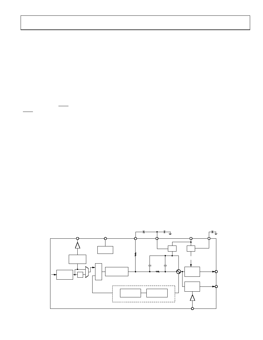
COMPONENT BLOCKS—OUTPUT PLL (PLL2)
PLL2 General Description
The output PLL (referred to as PLL2) consists of an optional
input reference doubler, reference divider, phase-frequency
detector (PFD), a partially integrated analog loop filter (see
Figure 27), an integrated voltage-controlled oscillator (VCO),
and a feedback divider. The VCO produces a nominal 3.0 GHz
signal with an output divider that is capable of division ratios of
3, 4, and 5.
The PFD of the output PLL drives a charge pump that increases,
decreases, or holds constant the charge stored on the loop filter
capacitors (both internal and external). The stored charge results
in a voltage that sets the output frequency of the VCO. The
feedback loop of the PLL causes the VCO control voltage to
vary in a way that phase locks the PFD input signals.
The gain of PLL2 is proportional to the current delivered by
the charge pump. The loop filter bandwidth is chosen to reduce
noise contributions from PLL sources that could degrade phase
noise requirements.
The output PLL has a VCO with multiple bands spanning a range
of 2.94 GHz to 3.1 GHz. However, the actual operating frequency
within a particular band depends on the control voltage that
appears on the loop filter capacitor. The control voltage causes
the VCO output frequency to vary linearly within the selected
band. This frequency variability allows the control loop of the
output PLL to synchronize the VCO output signal with the
reference signal applied to the PFD. Typically, the device
automatically selects the appropriate band as part of its
calibration process (invoked via the VCO control register
at Address 0x0F3, shown in Table 47).
N DIVIDER
TO DIST/
RESYNC
×2
PLL1_OUT
LDO
PLL_1.8V
LDO_DIV_M1
VDD3_VCO
VDD3_REF
LDO_VCO
DIVIDE-BY-
1, 2, 4, 8, 16
R2
DIVIDE-BY-
1, 2, 3...31
M1
DIVIDE-BY-
3, 4, 5,
DIVIDE-BY-4
PRESCALER
A/B
COUNTERS
CHARGE PUMP
7 BITS, 3.5A LSB
PFD
RZERO
RPOLE2
CPOLE1
CPOLE2
LF2_EXT_CAP
VDD3_PLL
PLL CORE
1.9V
TO DIST/
RESYNC
M2
DIVIDE-BY-
3, 4, 5,
AD9523-1
09
27
8-
0
23
Figure 27. Output PLL (PLL2) Block Diagram
相关PDF资料 |
PDF描述 |
|---|---|
| V150C5C100BF | CONVERTER MOD DC/DC 5V 100W |
| V150C5C100BL3 | CONVERTER MOD DC/DC 5V 100W |
| V150C5C100B3 | CONVERTER MOD DC/DC 5V 100W |
| V150C5C100B2 | CONVERTER MOD DC/DC 5V 100W |
| AD9512/PCBZ | BOARD EVAL FOR AD9512 |
相关代理商/技术参数 |
参数描述 |
|---|---|
| AD9523BCPZ | 功能描述:IC INTEGER-N CLCK GEN 72LFCSP RoHS:是 类别:集成电路 (IC) >> 时钟/计时 - 专用 系列:- 标准包装:28 系列:- 类型:时钟/频率发生器 PLL:是 主要目的:Intel CPU 服务器 输入:时钟 输出:LVCMOS 电路数:1 比率 - 输入:输出:3:22 差分 - 输入:输出:无/是 频率 - 最大:400MHz 电源电压:3.135 V ~ 3.465 V 工作温度:0°C ~ 85°C 安装类型:表面贴装 封装/外壳:64-TFSOP (0.240",6.10mm 宽) 供应商设备封装:64-TSSOP 包装:管件 |
| AD9523BCPZ-REEL7 | 功能描述:IC INTEGER-N CLCK GEN 72LFCSP RoHS:是 类别:集成电路 (IC) >> 时钟/计时 - 专用 系列:- 标准包装:28 系列:- 类型:时钟/频率发生器 PLL:是 主要目的:Intel CPU 服务器 输入:时钟 输出:LVCMOS 电路数:1 比率 - 输入:输出:3:22 差分 - 输入:输出:无/是 频率 - 最大:400MHz 电源电压:3.135 V ~ 3.465 V 工作温度:0°C ~ 85°C 安装类型:表面贴装 封装/外壳:64-TFSOP (0.240",6.10mm 宽) 供应商设备封装:64-TSSOP 包装:管件 |
| AD9524 | 制造商:AD 制造商全称:Analog Devices 功能描述:Jitter Cleaner and Clock Generator with 6 Differential or 13 LVCMOS Outputs |
| AD9524/PCBZ | 功能描述:BOARD EVAL FOR AD9524 RoHS:是 类别:编程器,开发系统 >> 评估演示板和套件 系列:- 标准包装:1 系列:PSoC® 主要目的:电源管理,热管理 嵌入式:- 已用 IC / 零件:- 主要属性:- 次要属性:- 已供物品:板,CD,电源 |
| AD9524BCPZ | 功能描述:IC INTEGER-N CLCK GEN 48LFCSP RoHS:是 类别:集成电路 (IC) >> 时钟/计时 - 专用 系列:- 标准包装:28 系列:- 类型:时钟/频率发生器 PLL:是 主要目的:Intel CPU 服务器 输入:时钟 输出:LVCMOS 电路数:1 比率 - 输入:输出:3:22 差分 - 输入:输出:无/是 频率 - 最大:400MHz 电源电压:3.135 V ~ 3.465 V 工作温度:0°C ~ 85°C 安装类型:表面贴装 封装/外壳:64-TFSOP (0.240",6.10mm 宽) 供应商设备封装:64-TSSOP 包装:管件 |
发布紧急采购,3分钟左右您将得到回复。